Welcome Here Shenzhen Mingjiada Electronics Co., Ltd.

sales@hkmjd.com

sales@hkmjd.com

Service Telephone:86-755-83294757
 Latest Information
 Home
/Company Dynamics
/
LTC6362CDD Differential Amplifier: 1ma Rail-to-Rail Input/Output Differential Op Amp
The LTC6362CDD is a low power, low noise differential operational amplifier optimized for driving low power SAR ADCs .Basic parametersModel: LTC6362CDDAmplifier type: DifferentialNumber of circuits: 1Output type: Differential, full swingPressure swi…
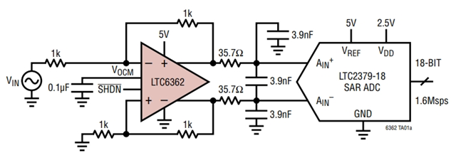
The LTC6362CDD is a low power, low noise differential operational amplifier optimized for driving low power SAR ADCs .

Basic parameters
Model: LTC6362CDD
Amplifier type: Differential
Number of circuits: 1
Output type: Differential, full swing
Pressure swing rate: 45V/µs
Gain-bandwidth product: 180 MHz
-3db bandwidth: 34 MHz
Current - Input bias: 75 nA
Voltage - Input compensation: 75 µV
Current - Power supply: 1mA
Voltage - Span (minimum) : 2.8V
Voltage - Span (maximum value) : 5.25V
Operating temperature: 0°C to 70°C
Installation type: Surface mount type
Package/Housing: 8-DFN
Description of LTC6362
The LTC6362CDD is a low-power, low-noise differential operational amplifier with rail-to-rail input and output swings, which has been optimized specifically for driving low-power SAR ADCs. The LTC6362CDD only absorbs 1mA of power supply current during active operation and features A shutdown mode in which current consumption is reduced to 70μA.
The amplifier can be configured to convert a single-ended input signal into a differential output signal and can operate in either inverting or non-inverting configurations.
The low offset voltage, low input bias current and a stable high-impedance configuration make this amplifier not only suitable for use as an ADC driver, but also in the forward signal link to convert a precise sensor signal into a balanced (differential) signal that can be processed in a noisy industrial environment.
The LTC6362CDD is available in a compact 3mm x 3mm 8-pin leadless DFN package and can operate within a temperature range of -40°C to 125°C, while ensuring compliance with specified performance indicators.
Application field
The LTC6362CDD is applicable to a variety of application fields, mainly including:
16-bit and 18-bit SAR ADC drivers
Single-ended to differential conversion
Low-power pipelined ADC driver
Differential line driver
Battery-powered instrument
In addition, the LTC6362CDD also has the following main features:
1mA power supply current
2.8V to 5.25V single power supply
Fully differential input and output
Maximum offset voltage of 200μV
Maximum input bias current of 260nA
Fast and stable: 550ns to 18-bit, 8VP-P output
Low distortion: -116dBc (at 1kHz, 8VP-P)
Rail-to-rail input and output
3.9nV/√Hz input reference noise
180MHz gain-bandwidth product
34 MHZ -3dB bandwidth
Low-power shutdown mode: 70μA
3mm x 3mm 8-pin DFN package
Immediately visit Mingjiada electronic official website (www.hkmjd.com), get LTC6362CDD products exclusive quotation!

Time:2025-09-10
![DS1302Z Clock Chip with Trickle Charging Using 3-Wire Serial Interface [ADI Products]](/upload/202509/10/202509101117227339.jpg)
Time:2025-09-10
![Supply ADI [ADUM2201ARWZ] dual-channel digital isolator, 5kV, 1Mbps, 25kV/µs CMTI 16-SOIC](/upload/202509/10/202509101100302758.jpg)
Time:2025-09-10

Time:2025-09-10
Contact Number:86-755-83294757
Enterprise QQ:1668527835/ 2850151598/ 2850151584/ 2850151585
Business Hours:9:00-18:00
E-mail:sales@hkmjd.com
Company Address:Room1239, Guoli building, Zhenzhong Road, Futian District, Shenzhen, Guangdong
CopyRight ©2022 Copyright belongs to Mingjiada Yue ICP Bei No. 05062024-12

Official QR Code
Links: