Welcome Here Shenzhen Mingjiada Electronics Co., Ltd.


sales@hkmjd.com
sales@hkmjd.com


Service Telephone:86-755-83294757
 Latest Information
 Home
/Company Dynamics
/
Home
/Company Dynamics
/
Analog Devices Introduces Wide Dynamic Range RF Power Detector — ADL5903ACPZN
Overview:The ADL5903ACPZN is a true root-mean-square response power detector with a 35 dB measuring range. The device provides low power performance with built-in ripple error transmission.The ADL5903 provides a solution for a wide range of high frequ…
Overview:
The ADL5903ACPZN is a true root-mean-square response power detector with a 35 dB measuring range. The device provides low power performance with built-in ripple error transmission.
The ADL5903 provides a solution for a wide range of high frequency systems requiring accurate signal power measurements. The device is powered by a single supply from 3.0V to 5.0V, can be easily used with only a few capacitors, and can be driven with a single end, or with a differential input using Barron. The on-chip matching network provides good return loss performance in the rated frequency range of the device. The ADL5903 operates in the 200 MHz to 6 GHz frequency range and supports input ranges from −30 dBm to +20 dBm.
The ADL5903 can be used to determine the true power of high frequency signals with complex modulation envelopes, including large crest factor signals such as GSM, CDMA, W-CDMA, TD-SCDMA and LTE modulated signals. The output is then proportional to the logarithm of the input RMS value. In other words, readings are presented directly in decibels and adjusted to approximately 35.5 mV/dB at 900 MHz.
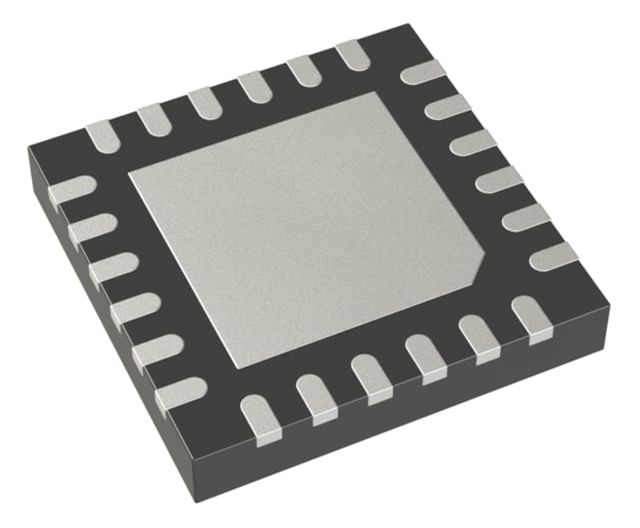
The ADL5903 operates with low power consumption, which is further reduced by disabling the mode. When the ADL5903 enters the off mode through a logic low on the ENBL pin, its power consumption is less than 100 μA. The ADL5903 is available in a 2 mm x 2 mm, 8-pin LFCSP package with a wide operating temperature range from −55°C to +125°C.
Main features of ADL5903:
Precise RMS to DC conversion (200 MHz to 6 GHz)
Measurement dynamic range: 35 dB
No ripple transfer function
Single-end input, compatible with 50 Ω signal sources
No external matching required
Linear dB output, adjusted to 35.5 mV/dB (900 MHz)
Waveform and modulation independent, such as:
GSM/CDMA/W-CDMA
/TD-SCDMA/LTE
Excellent temperature stability
The operating temperature ranges from −55°C to +125°C with 3.0V to 5.0V power supply
Low power consumption: 3 mA (3.0V to 5.0V supply)
8-pin, 2 mm x 2 mm LFCSP package
Applications:
• Power amplifier linearization/control loop
• Transmitter power control
Transmitter Signal Strength Indication (TSSI)
• RF instrumentation
• Wireless repeater
Functional block diagram:

If you have any needs, please call us:
Contact: Mr. Chen
Tel: +8613410018555
Email: sales@hkmjd.com
Time:2025-07-17

Time:2025-07-17
Time:2025-07-17

Time:2025-07-17
Contact Number:86-755-83294757
Enterprise QQ:1668527835/ 2850151598/ 2850151584/ 2850151585
Business Hours:9:00-18:00
E-mail:sales@hkmjd.com
Company Address:Room1239, Guoli building, Zhenzhong Road, Futian District, Shenzhen, Guangdong
CopyRight ©2022 Copyright belongs to Mingjiada Yue ICP Bei No. 05062024-12

Official QR Code
Links:


