Welcome Here Shenzhen Mingjiada Electronics Co., Ltd.

sales@hkmjd.com

sales@hkmjd.com

Service Telephone:86-755-83294757
 Latest Information
 Home
/Company Dynamics
/
Clock Buffer and Driver 8S89832AKILFT Introduction: 1:4 Differential to LVDS Fanout Buffer
DescriptionThe 8S89832AKILFT is a high-speed 1:4 differential to LVDS fan-out buffer. This device has been optimized for high speed and extremely low output skew, making it suitable for demanding applications such as SONET, 1 Gigabit and 10 Gigabit Et…
Description
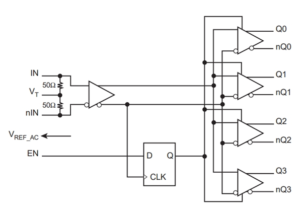
The 8S89832AKILFT is a high-speed 1:4 differential to LVDS fan-out buffer. This device has been optimized for high speed and extremely low output skew, making it suitable for demanding applications such as SONET, 1 Gigabit and 10 Gigabit Ethernet, as well as Fibre Channel.
Functional features
Differential input/output : 8S89832AKILFT supports differential signal transmission.
Logic type : low offset clock driver, suitable for high-speed signal transmission scenarios.
Its internally terminated differential input and VREF_AC pin allow other differential signal series (such as LVPECL, LVDS and SSTL) to be easily connected to the input with minimal use of external components. The 8S89832AKILFT also features an output enable pin, which can be used for system testing and debugging purposes. The 8S89832AKILFT is available in a small 3mm x 3mm 16-pin VFQFN package, making it highly suitable for space-constrained applications.

In addition, the 8S89832AKILFT has the following main features:
Four differential LVDS output pairs
The IN and nIN input pairs can accept the following differential input levels: LVPECL, LVDS, and SSTL
The 50Ω internal input terminal of VT
Maximum output frequency: 2GHz
Output skew: 25ps (maximum)
Inter-part skew: 200ps (maximum)
Propagation delay: 550ps (maximum)
Additional phase jitter, RMS: 0.09ps (typical value)
Full 2.5V power supply mode
Ambient operating temperature: -40°C to 85°C
Lead-free (RoHS 6) packaging is adopted
Application scenarios
The 8S89832AKILFT clock buffer is mainly applied in scenarios such as clock signal distribution and high-speed data transmission systems that require low offset and high stability.
The specific parameters of 8S89832AKILFT are as follows:
Type: Fan-out buffer (allocated)
Number of circuits: 1
Ratio - Input: Output: 1:4
Differential - Input: Output: Yes/Yes
Input: LVDS, LVPECL, SSTL
Output: LVDS
Frequency - Maximum: 2 GHz
Voltage - Power supply: 2.375V to 2.625V
Operating temperature: -40°C to 85°C
Installation type: Surface mount type
Package/Housing: 16-VFQFPN (3x3)
For more information
For 8S89832AKILFT clock buffers, please visit www.hkmjd.com.

Time:2025-08-28

Time:2025-08-28
![[STBR3012L2Y] Automotive High Voltage Rectifier for Bridge Applications, Diode 1200 V 30A](/upload/202508/28/202508281413132053.png)
Time:2025-08-28

Time:2025-08-28
Contact Number:86-755-83294757
Enterprise QQ:1668527835/ 2850151598/ 2850151584/ 2850151585
Business Hours:9:00-18:00
E-mail:sales@hkmjd.com
Company Address:Room1239, Guoli building, Zhenzhong Road, Futian District, Shenzhen, Guangdong
CopyRight ©2022 Copyright belongs to Mingjiada Yue ICP Bei No. 05062024-12

Official QR Code
Links: