Welcome Here Shenzhen Mingjiada Electronics Co., Ltd.

sales@hkmjd.com

sales@hkmjd.com

Service Telephone:86-755-83294757
 Latest Information
The 8SLVD2104NBGI launched by Renesas is a high-performance differential dual-channel LVDS ffan buffer with a maximum input clock frequency of up to 2GHz. It is specifically designed for ffan out high-frequency, extremely low additional phase noise cl…
The 8SLVD2104NBGI launched by Renesas is a high-performance differential dual-channel LVDS ffan buffer with a maximum input clock frequency of up to 2GHz. It is specifically designed for ffan out high-frequency, extremely low additional phase noise clock and data signals.
Core parameters
Type: Fan-out buffer (allocated)
Number of circuits: 2
Ratio - Input: Output: 1:4
Differential - Input: Output: None/None
Input: LVDS, LVPECL
Output: LVDS
Frequency - Maximum: 2 GHz
Voltage - Power supply: 2.375V to 2.625V
Operating temperature: -40°C to 85°C
Installation type: Surface mount type
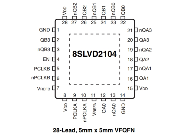
Packaging/Housing: 28-WFQFN

Introduction
The 8SLVD2104NBGI device is a high-performance differential dual-channel 1:4 LVDS fan-out buffer. This device is designed for fan-out high-frequency, extremely low additional phase noise clocks and data signals. The 8SLVD2104NBGI is characterized by being powered by a 2.5V power supply. The guaranteed output-to-output and part-to-part skew characteristics make the 8SLVD2104NBGI an ideal choice for clock distribution applications that require clear performance and repeatability. Two independent buffers are provided, each with four low-skew outputs. The integrated bias voltage generator enables single-ended signals to be easily connected to the device input. The 8SLVD2104NBGI has been optimized for low power consumption and low additional phase noise.
Main features
Two 1:4, low skew, low additional jitter LVDS fan-out buffers
Two differential clock inputs
The differential pair can accept the following differential input levels: LVDS and LVPECL
Maximum input clock frequency: 2GHz
Output group skew: 35ps (maximum)
Propagation delay: 300ps (maximum)
Low additional RMS phase jitter, 156.25MHz (10kHz to 20MHz) : 105fs (maximum)
2.5V power supply voltage
Lead-free (RoHS 6) 28-pin VFQFN package
Ambient operating temperature: -40 °C to 85 °C
Typical applications
The 8SLVD2104NBGI clock buffer is specifically designed for systems that require precise clock distribution, such as high-speed data transmission, video processing, and high-precision clock networks. It can effectively reduce signal loss and ensure multi-node synchronization.
Supply information
For 8SLVD2104NBGI clock buffer, please visit www.hkmjd.com.

Time:2025-08-28

Time:2025-08-28
![[STBR3012L2Y] Automotive High Voltage Rectifier for Bridge Applications, Diode 1200 V 30A](/upload/202508/28/202508281413132053.png)
Time:2025-08-28

Time:2025-08-28
Contact Number:86-755-83294757
Enterprise QQ:1668527835/ 2850151598/ 2850151584/ 2850151585
Business Hours:9:00-18:00
E-mail:sales@hkmjd.com
Company Address:Room1239, Guoli building, Zhenzhong Road, Futian District, Shenzhen, Guangdong
CopyRight ©2022 Copyright belongs to Mingjiada Yue ICP Bei No. 05062024-12

Official QR Code
Links: