Welcome Here Shenzhen Mingjiada Electronics Co., Ltd.

sales@hkmjd.com

sales@hkmjd.com

Service Telephone:86-755-83294757
 Latest Information
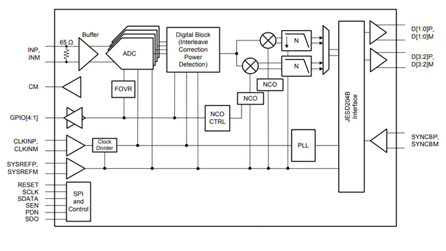
The ADC31RF80 is designed for high signal-to-noise ratio (SNR) and provides -155dBFS/Hz noise spectral density and dynamic range over a large input frequency range.
Overview:
The ADC31RF80IRMP is a 14-bit 3GSPS RF sampling broadband receiver and feedback integrated circuit with input frequencies up to 4GHz and above. The ADC31RF80 is designed for a high signal-to-noise ratio (SNR) and provides noise spectral density of -155dBFS/Hz over a large input frequency range as well as dynamic range. Buffered analog inputs with on-chip terminals provide uniform input impedance over the entire wide frequency range and minimize sampling and retention of burr pulse energy. The device contains a dual-band digital downconverter (DDC) with up to three independent 16-bit numerical control oscillators (NCO) per DDC for phase-coherent hopping. Supports JESD204B serial interface with deterministic latency based on subclass 1, using data rates up to 12.5Gbps with up to 4 channels. The ADC31RF80 has an industrial temperature range of -40 °C to +85°C.

Features:
14-bit 3GSPS ADC
Noise base: -155dBFS/Hz
Rf input support up to 4.0GHz
Aperture jitter: 90fS
Spectrum performance (fIN=900MHz, -2dbfs) :
SNR: 61.4dBFS
SFDR: 71dBc HD2, HD3
SFDR: 76dBc worst spurious
Spectrum performance (fIN=1.85GHz, -2dbfs) :
SNR: 58.5dBFS
SFDR: 65dBc HD2, HD3
SFDR: 75dBc worst spurious
On-chip digital downconverter:
Up to 2 DDC (dual band mode)
Up to 3 separate Ncos per DDC
On-chip input clamp for overvoltage protection
Programmable on-chip power detector with alarm pin support for AGC
On-chip dither
On-chip input terminal
Input full scale: 1.35VPP
Supports multi-chip synchronization
JESD204B Interface:
Deterministic delay based on subclass 1
4-channel support (12.5Gbps)
Total power dissipation: 3.2W (at 3.0GSPS)
72-pin VQFN package (10mm×10mm)
Applications:
Multi-carrier GSM cellular infrastructure base station
Telecommunication receiver
DPD observation receiver
Return receiver
Rf Repeaters and distributed antenna systems

Time:2025-07-11

Time:2025-07-11

Time:2025-07-11

Time:2025-07-11
Contact Number:86-755-83294757
Enterprise QQ:1668527835/ 2850151598/ 2850151584/ 2850151585
Business Hours:9:00-18:00
E-mail:sales@hkmjd.com
Company Address:Room1239, Guoli building, Zhenzhong Road, Futian District, Shenzhen, Guangdong
CopyRight ©2022 Copyright belongs to Mingjiada Yue ICP Bei No. 05062024-12

Official QR Code
Links: