Welcome Here Shenzhen Mingjiada Electronics Co., Ltd.

sales@hkmjd.com

sales@hkmjd.com

Service Telephone:86-755-83294757
 Latest Information
 Home
/Company Dynamics
/
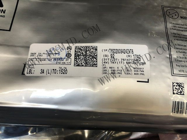
[TI] C64x + Fixed Point DSP-TMS320C6424ZWT6 NFBGA (ZWT) Digital Signal Processor
The TMS320C6424ZWT6 device is a C64x+ fixed-point DSP - up to 600MHz, 16/8-bit EMIFA, 32/16-bit DDR2, SDRAM.
The TMS320C6424ZWT6 device is a C64x+ fixed-point DSP - up to 600MHz, 16/8-bit EMIFA, 32/16-bit DDR2, SDRAM.
Instructions:
The TMS320C6424ZWT6 device is based on TI's third generation high-performance Advanced VelociTI Ultra-Long Instruction Word (VLIW) architecture and is the highest performing fixed-point DSP product in the TMS320C6000™ DSP platform.
With performance of up to 4.8 billion instructions per second (MIPS) at 600 MHz clock rates, the C64x+ core provides a solution to high performance DSP programming challenges. The DSP core has the operational flexibility of a high-speed controller and the digital capability of an array processor.

Parameters:
Core: C64x+
Type: Fixed point
Interface: EBI/EMI, HPI, I2C, McASP, McBSP, UART, 10/100 Ethernet MAC
Clock rate: 600MHz
Non-volatile memory: ROM (64kB)
On-chip RAM: 240kB
Voltage - I/O: 1.8V, 3.3V
Voltage - core: 1.05V, 1.20V
Operating temperature: 0°C ~ 90°C (TJ)
Mounting type: Surface mount type
Package/housing: 361-LFBGA
Supplier Package: 361-NFBGA (16x16)
Applications:
telegraphy
Audio frequency
Industrial application
Features:
High Performance Digital Signal Processor (C6424)
2.5 nanosecond, 2 nanosecond, 1.67 nanosecond and 1.43 nanosecond instruction cycle times
400, 500, 600 MHz C64x+ Clock rate
Eight 32-bit C64x+ instructions/cycles
3200, 4000, 48005600 MIPS
Fully software compatible with the C64x
Business and automotive (Q or S suffix) grades
Low power equipment (L suffix)
Velociti.2 Extends the VelociTI Advanced Ultra-Long Instruction Word (VLIW)TMS 320 c 64 x+DSP kernel
Eight highly independent functional units with VelociTI.2 extensions:
Six ALUs (32/40 bits) support single 32-bit, double 16-bit, or four-8-bit arithmetic operations per clock cycle
Two multipliers support four 16 × 16-bit multiplications (32-bit results) or eight 8 × 8-bit multiplications (16-bit results) per clock cycle
Load storage architecture with inconsistent support
64 32-bit general-purpose registers
Instruction packaging reduces code
All instructions are conditional
Other C64x+ enhancements
Protected mode operation
Exception support for error detection and program redirection
Hardware support for mode cycle autofocus module operation
C64x+ instruction set features
Bytes addressable (8/16/32/64 bit data)
8-bit overflow protection
Bit field extraction, setting, and clearing
Standardization, saturation, bit counting
VelociTI.2 Added orthogonality
C64x+ Extension
Reduced 16-bit instruction
Additional instructions to support complex multiplication
C64x+ L1/L2 memory architecture
256K bit (32K bytes)L1P program RAM/ Cache [Flexible allocation]
640 kilobits (80 kilobytes)L1D Data RAM/ Cache [Flexible allocation]
1M bit (128K bytes)L2 Unified Mapped RAM/ Cache [Flexible allocation]
End order: Supports small end order and large end order
External Memory Interface (EMIFs)
32-bit DDR2 SDRAM memory controller with 256M bytes of address space (1.8V I/O)
Supports buses up to 333 MHz(data rate) and interfaces with DDR2-400 SDRAM
Asynchronous 16-bit wide EMIF (EMIFA) with an address range of up to 128 MB
Flash interface
NOR(8/16 bit wide data)
NAND(8/16 bit wide data)
Enhanced Direct Memory Access (EDMA) Controller (64 independent channels)
Two 64-bit universal timers (each configurable as two 32-bit timers)
A 64 bit watchdog timer
Two UARTs(one with RTs and CTS flow control)
Master/slave internal integrated circuit (I2C bus)
Two multi-channel buffered serial ports (McBSPs)
I2S and TDM
AC97 audio codec interface
vigor
Standard Voice Codec Interface (AIC12)
Telecommunication interface - ST bus, H-100
128 channel mode
Multichannel Audio Serial Port (McASP0)
Four serializers and SPDIF (DIT) mode
16-bit Host Port Interface (HPI)
32-bit 33 MHz 3.3V Peripheral Component Interconnect (PCI) master/slave interface
10/100 Mb/s Ethernet MAC (EMAC)
Complies with IEEE 802.3 standard
Supports multiple media independent interfaces (MII, RMII)
Manage data input/output (MDIO) modules
VLYNQ Interface (FPGA interface)
Three way pulse width modulator (PWM) output
On-chip ROM boot loader
Separate power saving mode
Flexible PLL clock generator
Compatible with IEEE-1149.1 (JTAG) boundary scan
Up to 111 general purpose I/O (GPIO) pins (reusable with other device functions)
Packaging:
361 lead free PBGA package (ZWT suffix), 0.8mm ball pitch
376 Pin plastic BGA package (ZDU suffix), 1.0mm ball pitch
0.09 micron /6 layer Copper Metal Process (CMOS)
3.3V and 1.8V input/output, 1.2V internal (-7/-6/-5/-4/-Q6/-Q5/-Q4)
3.3V and 1.8V input/output, 1.05V internal (-7/-6/-5/-4/-L/-Q5)

Time:2025-07-08

Time:2025-07-08

Time:2025-07-07

Time:2025-07-07
Contact Number:86-755-83294757
Enterprise QQ:1668527835/ 2850151598/ 2850151584/ 2850151585
Business Hours:9:00-18:00
E-mail:sales@hkmjd.com
Company Address:Room1239, Guoli building, Zhenzhong Road, Futian District, Shenzhen, Guangdong
CopyRight ©2022 Copyright belongs to Mingjiada Yue ICP Bei No. 05062024-12

Official QR Code
Links: