Welcome Here Shenzhen Mingjiada Electronics Co., Ltd.

sales@hkmjd.com

sales@hkmjd.com

Service Telephone:86-755-83294757
 Latest Information
 Home
/Company Dynamics
/
TMS320VC5503PGE Low Power C55x Fixed Point DSP-Up to 200MHz _ New Supply _ TI Processors
The TMS320VC5503PGE is a low-power C55x fixed-point DSP - up to 200MHz.Product: TMS320VC5503PGEType: C55x fixed-point DSPClock frequency: 200MHzPackage: LQFP-144Description:TMS320VC5503 fixed-point digital signal processor (DSP) is based on TMS320C55x…
The TMS320VC5503PGE is a low-power C55x fixed-point DSP - up to 200MHz.
Product: TMS320VC5503PGE
Type: C55x fixed-point DSP
Clock frequency: 200MHz
Package: LQFP-144
Description:
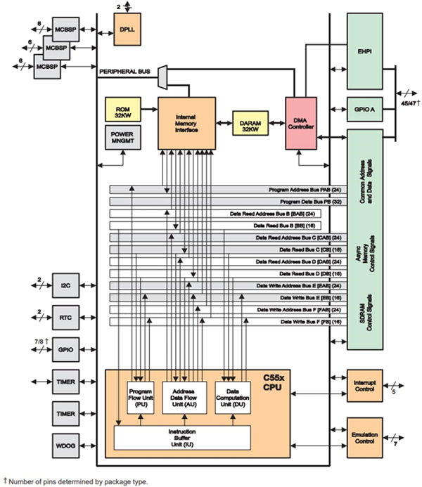
TMS320VC5503 fixed-point digital signal processor (DSP) is based on TMS320C55x DSP CPU processor core. By enhancing parallel capabilities and reducing power consumption across the board, the C55x DSP architecture delivers high performance and low power consumption. The CPU supports an internal bus architecture, which includes a program bus, three data read buses, two data write buses, and additional buses dedicated to peripheral and DMA operations. These buses can perform up to three data reads and two data writes in a single cycle. In parallel, DMA controllers can perform up to two data transfers per cycle, independent of CPU operation.
The 64K byte on-chip memory on the TMS320VC5503 is sufficient to meet the needs of many small handheld appliances, portable personal devices, gaming devices, and personal medical care devices. Many of these appliances typically require 64K bytes or less of on-chip memory, and more than 60-70% of the time they need to operate in standby mode.
The TMS320C5503 peripheral set includes an external memory interface (EMIF) for seamless access to asynchronous memory such as EPROM and SRAM, as well as high-speed high-density memory such as synchronous DRAM. Other peripherals include a real-time clock, a watchdog timer, and an I2C multi-master-slave interface.
Functional block diagram:
Features:
High performance, low power, fixed-point TMS320C55™ digital signal processor
Instruction cycle time: 9.26ns, 6.95ns, 5ns
Clock speed: 108MHz, 144MHz, 200MHz
Execute one or two instructions per cycle
Double multiplier [up to 400 million multiplications per second (MMACS)]
Two arithmetic/Logic units (ALU)
Three internal data/operand read buses and two internal data/operand write buses
32K x 16-bit on-chip RAM, inclusive
64KB Dual access RAM (DARAM), 8 blocks 4Kx16 bits
64KB Single Wait State on-chip ROM (32K x 16-bit)
8M x 16 bit maximum addressable external memory space (synchronous DRAM)
16-bit external parallel bus memory, either supported
External memory interface (EMIF) with GPIO functionality and seamless connectivity
Asynchronous Static RAM(SRAM)
Asynchronous EPROM
Synchronous DRAM (SDRAM)
16-bit Parallel Enhanced Host Port Interface (EHPI) with GPIO capability
Programmable low power control of six device function areas
Simulation logic based on scan on chip
On-chip peripherals
Two 20-bit timers
Watchdog timer
6-channel Direct Memory access (DMA) controller
Three multi-channel buffered serial Ports (McBSP)
Programmable phase-locked loop (PLL) clock generator
Seven (LQFP) or eight (BGA) Universal I/O (GPIO) pins and one universal Output pin (XF)
Internal integrated circuit (I2C) multi-master/slave interface
Real-time clock (RTC) with crystal input, independent clock domain, and independent power supply
IEEE Std 1149.1 (JTAG) boundary scan logic
encapsulation
144 Pin Thin Square Flat (LQFP) package (PGE suffix)
179 Pin MicroStar BGA™ (Ball Grid Array) (GHH and ZHH suffixes)
1.2V core (108MHz), 2.7V to 3.6V I/O
1.35V core (144MHz), 2.7V to 3.6V I/O
1.6V core (200MHz), 2.7V to 3.6V I/O
Time:2025-07-07
Time:2025-07-07
Time:2025-07-07
Time:2025-07-07
Contact Number:86-755-83294757
Enterprise QQ:1668527835/ 2850151598/ 2850151584/ 2850151585
Business Hours:9:00-18:00
E-mail:sales@hkmjd.com
Company Address:Room1239, Guoli building, Zhenzhong Road, Futian District, Shenzhen, Guangdong
CopyRight ©2022 Copyright belongs to Mingjiada Yue ICP Bei No. 05062024-12

Official QR Code
Links: