Welcome Here Shenzhen Mingjiada Electronics Co., Ltd.

sales@hkmjd.com

sales@hkmjd.com

Service Telephone:86-755-83294757
 Latest Information
Overview:The TMS320VC5409AGWS12 fixed-point digital signal processor (DSP) is based on the advanced and improved Harvard architecture, with one program memory bus and three data memory buses. The processor provides a highly parallel arithmetic logic u…
Overview:
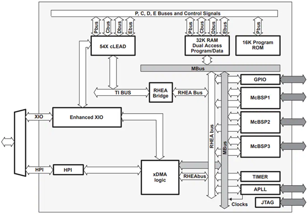
The TMS320VC5409AGWS12 fixed-point digital signal processor (DSP) is based on the advanced and improved Harvard architecture, with one program memory bus and three data memory buses. The processor provides a highly parallel arithmetic logic unit (ALU), application-specific hardware logic, on-chip memory, and other on-chip peripherals. The operational flexibility and speed of the Texas Instruments TMS320VC5409A is based on a highly specialized instruction set.
Separate program and data Spaces allow simultaneous access to program instructions and data, providing a high degree of parallelism. Two read operations and one write operation can be performed in one cycle. Instructions with parallel storage and application of specific instructions can take full advantage of this architecture. In addition, data can be transferred between data and program space. This parallel technology enables powerful arithmetic, logical, and bit-operated operations that can be performed in a single machine cycle. The device also includes control mechanisms for managing interruptions, repetitive operations, and functional calls.
Product: TMS320VC5409AGWS12
Core: C54x
Clock frequency: 20 MHz
Package: BGA-144
Functional block diagram:
Features:
Advanced Multibus architecture with three separate 16-bit data memory buses and one program memory bus
A 40-bit arithmetic logic unit (ALU) consisting of a 40-bit barrel shifter and two separate 40-bit accumulators
17-× 17-bit parallel frequency multiplier coupled to a 40-bit private network extender for non-pipelined single-cycle multiply/add (MAC) operations
Compare, Select, and store units (CSSUs) to add/compare Viterbi operators' selections
Index encoder, used to calculate the index value of the 40-bit accumulator value in one cycle
Two address generators with eight secondary registers and two secondary register algorithm units (ARAU)
A data bus with a bus bracket function
Extended addressing mode for 8M\xD7 × 16-bit maximum addressable external program space
32K x 16-bit on-chip RAM, inclusive
Four 8K\xD7 16-bit on-chip dual-access program/data RAM
16K\xD7× 16-bit on-chip ROM, configured for program memory
Enhanced External Parallel Interface (XIO2)
Single instruction repetition and block repetition operations for program code
Block-memory-move instructions for better programming and data management
Instruction with 32-bit long word operand
An instruction read with two or three operands
Arithmetic instruction with parallel storage and parallel load
Conditional storage instruction
Interrupt quick return
On-chip peripherals
Software programmable wait state generator and programmable group switching
Programmable on-chip phase-locked loop (PLL) clock generator with internal oscillator or external clock source
A 16-bit timer
6-channel Direct Memory access (DMA) controller
Three multi-channel buffered serial Ports (McBSP)
8/16 bit Enhanced Parallel Host Port Interface (HPI8/16)
Power control with IDLE1, IDLE2, and IDLE3 instructions with power down mode
CLKOUT Turns off control to disable CLKOUT
Scan-on-chip based simulation logic, IEEE Std 1149.1 (JTAG) Boundary Scan logic
144 Pin Ball Grid Array (BGA) (GGU suffix)
144 Pin Thin Square Flat Package (LQFP) (PGE suffix)
6.25ns single-cycle fixed-point instruction execution time (160 MIPS)
8.33ns single-cycle fixed-point instruction execution time (120 MIPS)
3.3V I/O supply voltage (160 and 120 MIPS)
1.6V core supply voltage (160 MIPS)
1.5V core supply voltage (120 MIPS)
Time:2025-07-07
Time:2025-07-07
Time:2025-07-07
Time:2025-07-07
Contact Number:86-755-83294757
Enterprise QQ:1668527835/ 2850151598/ 2850151584/ 2850151585
Business Hours:9:00-18:00
E-mail:sales@hkmjd.com
Company Address:Room1239, Guoli building, Zhenzhong Road, Futian District, Shenzhen, Guangdong
CopyRight ©2022 Copyright belongs to Mingjiada Yue ICP Bei No. 05062024-12

Official QR Code
Links: