Welcome Here Shenzhen Mingjiada Electronics Co., Ltd.

sales@hkmjd.com

sales@hkmjd.com

Service Telephone:86-755-83294757
 Latest Information
 Home
/Company Dynamics
/
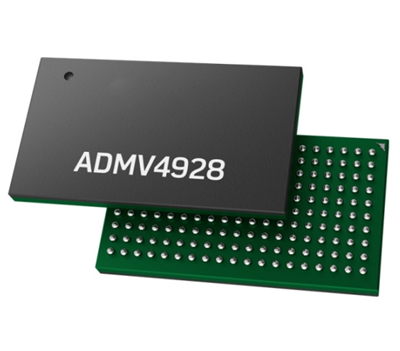
Supply (ADI) ADMV4928BBCZ 37.0 GHz to 43.5 GHz Transmit/Receive Dual Polarization Beamformer
The ADMV4928BBCZ is a Silicon on Insulator (SOI), 37.0 GHz to 43.5 GHz, mmW 5G beamformers. The RF integrated circuit (RFIC) is highly integrated and contains 16 separate transmit and receive channels. The ADMV4928 supports eight horizontally and eigh…
The ADMV4928BBCZ is a Silicon on Insulator (SOI), 37.0 GHz to 43.5 GHz, mmW 5G beamformers. The RF integrated circuit (RFIC) is highly integrated and contains 16 separate transmit and receive channels. The ADMV4928 supports eight horizontally and eight vertically polarized antennas with separate RFV and RFH inputs/outputs.
The ADMV4928 can be programmed through a 3-wire or 4-wire serial port interface (SPI). The integrated Low Voltage Difference (LDO) regulator generates a 1.0V supply voltage for the SPI circuit, reducing the number of power domains required.
The ADMV4928 offers a variety of SPI modes for fast startup and control during normal operation. The amplitude and phase of each channel can be set individually or multiple channels can be programmed simultaneously using on-chip memory to achieve beamforming. On-chip memory can store up to 2048 beam positions, which can be allocated for horizontal and vertical channels in transmit mode or receive mode.

Product: ADMV4928BBCZ
Package: BGA-239
Type: Beamformers
Features:
RF range: 37.0GHz to 43.5GHz
Output power >11.5 dBm (3% EVM, 400 MHz 64 QAM 5G NR waveform, only 340 mW per channel)
Complete features with 5G NR, WiFi 5, WiFi 6 and CPE UL waveforms
EVM performance is not degraded at 5G NR wide channel bandwidth
16 configurable transmit and receive channels
Dual polarization, 8 horizontal and 8 vertical channels
Fast TDD switching time (using TRX_x pin)
Matches 50 Ω, single-ended RF inputs and outputs
Single transmitter channel power detector and temperature sensor
Integrated single receive channel overload detection circuit
High-resolution, 6-bit VM is used to control phase
High resolution, 6 - and 5-bit DVGA are used to control amplitude
The memory is used for 2048 shared transmit and receive beam locations
NVM is used for phase and gain calibration
Dual power supply required: 1.8V and 1.2V (integrated on-chip LDO regulator provides 1.0V voltage)
3-wire or 4-wire SPI supports SPI clock speeds up to 133 MHz (see AN-2074 Application Notes ADMV4928 Application Notes)
239 pin, 10 mm x 7 mm CSP_BGA package
Applications:
• mmW 5G applications
• Broadband communication
![Renesas Electronics [MCU Chip] R5F21334CNFP 16-bit Microcontroller with R8C CPU Core](/upload/202507/05/202507051536017382.jpg)
Time:2025-07-05
![[Silicon Labs Original] EFM32GG230F512G-E-QFN64 High-Performance 32-Bit Microcontroller](/upload/202507/05/202507051518081938.jpg)
Time:2025-07-05

Time:2025-07-05

Time:2025-07-05
Contact Number:86-755-83294757
Enterprise QQ:1668527835/ 2850151598/ 2850151584/ 2850151585
Business Hours:9:00-18:00
E-mail:sales@hkmjd.com
Company Address:Room1239, Guoli building, Zhenzhong Road, Futian District, Shenzhen, Guangdong
CopyRight ©2022 Copyright belongs to Mingjiada Yue ICP Bei No. 05062024-12

Official QR Code
Links: