Welcome Here Shenzhen Mingjiada Electronics Co., Ltd.

sales@hkmjd.com

sales@hkmjd.com

Service Telephone:86-755-83294757
 Latest Information
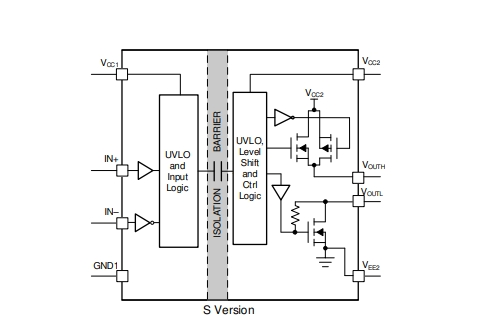
The UCC5320SCDWV is a single channel isolated gate driver designed to drive MOSFETs, IGBTs and SiC MOSFETs. The UCC53x0S provides a separate output to control the rise and fall times respectively.
Mingjiada Electronics sells original (UCC5320 SCDWV) TI single-channel isolated gate driver
Product description
The UCC5320SCDWV is a single channel isolated gate driver designed to drive MOSFETs, IGBTs and SiC MOSFETs. The UCC53x0S provides a separate output to control the rise and fall times respectively.
The UCC53x0 is available in a 4mm SOIC-8 (D) or 8.5mm SOIC-8 (DWV) package and can support isolation voltages up to 3kVRMS and 5kVRMS, respectively. With these various options, the UCC53x0 series is ideal for motor drivers and industrial power supplies.
Compared to optical couplers, the UCC53x0 series offers lower interdevice offset, lower propagation delay, higher operating temperature, and higher CMTI.
Features
• Feature options
- Separate output (UCC53x0S)
- UVLO (UCC53x0E) based on GND2
- Miller Clamp Option (UCC53x0M)
• 8-pin D (4mm creepage) and DWV (8.5mm creepage) packages
• 60ns (typical value) propagation delay
• Minimum CMTI of 100kV/μs
• Fence life > 40 years
• 3V to 15V input power supply voltage
• Driver supply voltage up to 33V
- 8V and 12V UVLO options
• The input pin has a negative 5V voltage handling capability
• Safety related certifications:
- 7,000 VPK isolated DWV (plan) and 4242VPK isolated D according to DIN V VDE V 0884-11:20017-01 and DIN EN 61010-1
- 5000VRMS DWV and 3000VRMS D isolation grades up to 1 minute in compliance with UL 1577
- CQC certification in accordance with GB4943.1-2011 D and DWV standards (program)
• CMOS input
• Operating temperature: -40°C to +125°C
Applications
• Motor driver
• High voltage DC to DC converter
• UPS and PSU
• HEV and EV power modules
• Photovoltaic inverter
Functional block diagram

![Supply [TI] TPS7B7702QPWPRQ1 Dual-Channel Adjustable Antenna Low-Dropout Voltage Regulator](/upload/202508/09/202508091412024980.jpg)
Time:2025-08-09

Time:2025-08-09

Time:2025-08-09

Time:2025-08-09
Contact Number:86-755-83294757
Enterprise QQ:1668527835/ 2850151598/ 2850151584/ 2850151585
Business Hours:9:00-18:00
E-mail:sales@hkmjd.com
Company Address:Room1239, Guoli building, Zhenzhong Road, Futian District, Shenzhen, Guangdong
CopyRight ©2022 Copyright belongs to Mingjiada Yue ICP Bei No. 05062024-12

Official QR Code
Links: