Welcome Here Shenzhen Mingjiada Electronics Co., Ltd.


sales@hkmjd.com
sales@hkmjd.com


Service Telephone:86-755-83294757
 Latest Information
 Home
/Company Dynamics
/
Home
/Company Dynamics
/
[ADI] ADMV1128ABBCZ 24GHz to 29.5GHz 5G microwave upconverter and downconverter
The [ADI] ADMV1128ABBCZ is an isolator on-silicon (SOI), microwave, up-converter, and down-converter optimized for 5G RF designs operating in the 24GHz to 29.5GHz frequency range.
Product description
The ADMV1128ABBCZ is an isolator on Silicon (SOI), microwave, upconverter, and downconverter, and is optimized for 5G RF designs operating in the frequency range of 24GHz to 29.5GHz.

Both upconverter and downconverter offer two frequency conversion modes. One mode is the conversion from and/or to a single-ended or complex intermediate frequency (IF) signal, which is then mixed through the on-chip 90° IF, called the IF mode.
The other mode is a direct conversion from and/or to differential baseband in-phase/orthogonal (I/Q) inputs and outputs, called baseband mode. The I/Q baseband output common-mode voltage is programmable between 0V and 1.5V. SPI provides fine-tuning of orthogonal phases to optimize I/Q demodulation performance.
peculiarity
An up converter (transmitter), a down converter (receiver) and an LO chain with a 2 x or 4 x multiplier are integrated in the chip
Radio frequency range: 24GHz to 29.5GHz
LO input frequency range: 8GHz to 15GHz in x2 mode and 5GHz to 7.5GHz in x4 mode
Two operating modes of upconverter and downconverter
Differential baseband I/Q direct conversion (Baseband mode)
Complex IF operation with optional in-chip mixing (IF mode)
The programmable baseband output common-mode voltage in receive mode ranges from 0.7V to 1.5V, which can be set by SPI or physical pin
The programmable mixer gate voltage ADAPTS to a common mode of baseband input from 0V to 1.5V in send mode
Matched 50Ω impedance, single-ended RF input and output, and RF switching ports
Matched 50Ω impedance, single-ended LO input
Low phase variation and gain control
Up-conversion mode
Sideband suppression and carrier feedthrough optimization
Envelope detector for LO feed-through calibration
Down-conversion mode
Image suppression and I/Q imbalance optimization
Baseband I/Q DC offset correction
Receiver mixer power detector for receiver gain setting
LO chain characteristics
Variable gain to accommodate various LO drive intensity values
360° phase shifter for LO synchronization
Programmable LO harmonic suppression filter
I/Q phase correction
Fast TDD switching times with external pins
Calibration probe for array calibration
Fully programmable via a 3-wire or 4-wire SPI interface and compatible with the ADMV4828 interface
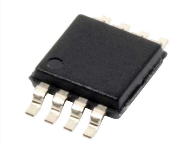
6mm x 6.5mm, BGA package (see overall dimensions section)
Applications
• Millimeter wave 5G applications
• Point-to-point microwave RF
• Radar and electronic warfare systems
• Instrumentation and automatic test equipment (ATE)
Time:2025-07-18
Time:2025-07-18
Time:2025-07-18

Time:2025-07-18
Contact Number:86-755-83294757
Enterprise QQ:1668527835/ 2850151598/ 2850151584/ 2850151585
Business Hours:9:00-18:00
E-mail:sales@hkmjd.com
Company Address:Room1239, Guoli building, Zhenzhong Road, Futian District, Shenzhen, Guangdong
CopyRight ©2022 Copyright belongs to Mingjiada Yue ICP Bei No. 05062024-12

Official QR Code
Links:


