Welcome Here Shenzhen Mingjiada Electronics Co., Ltd.

sales@hkmjd.com

sales@hkmjd.com

Service Telephone:86-755-83294757
 Latest Information
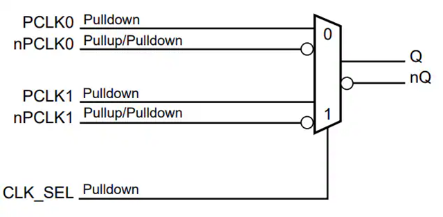
The 854S01AKILF is a clock multiplexer chip launched by Renesas, featuring a 16-VFQFN package. It supports 2:1 differential input/output conversion and has a maximum frequency of up to 2.5GHz. The following is the specific parameter information of 854…
The 854S01AKILF is a clock multiplexer chip launched by Renesas, featuring a 16-VFQFN package. It supports 2:1 differential input/output conversion and has a maximum frequency of up to 2.5GHz. The following is the specific parameter information of 854S01AKILF:
Type: Multiplexer
Number of circuits: 1
Ratio - Input: Output: 2:1
Differential - Input: Output: Yes/Yes
Input: LVDS, LVPECL
Output: LVDS
Frequency - Maximum: 2.5 GHz
Voltage - Power supply: 3.135V to 3.465V
Operating temperature: -40°C to 85°C
Installation type: Surface mount type
Package/Housing: 16-VFQFN
Description
The 854S01AKILF is designed as a high-performance 2:1 differential to LVDS multiplexer, capable of performing differential conversion by accepting differential inputs at LVPECL, LVDS or CML levels. The 854S01AKILF uses a resistive bias network on nPCLK0 and nPCLK1 to convert LVCMOS/LVTTL input signals to LVDS levels. This device features a 2:1 LVDS MUX and one LVDS output pair, with a maximum input/output frequency of 2.5GHz, an RMS additional phase jitter of 0.06ps (typical value), and a propagation delay of 600ps (maximum value). The 854S01AKILF multiplexer is available in a small 3mm x 3mm 16-VFQFN package and is highly suitable for circuit boards with limited space.

Main features
2:1 LVDS multiplexer
A pair of LVDS outputs
It can accept two differential clock inputs (LVPECL, LVDS, CML).
Maximum input/output frequency of 2.5GHz
The LVCMOS/LVTTL input signal is converted to LVDS level by using a resistive bias network on nPCLK0 and nPCLK1
0.06ps (typical value) RMS with additional phase jitter
600ps (maximum) propagation delay
The deviation between parts is 350ps (maximum)
Full 3.3V power supply mode
Ambient operating temperature: -40°C to 85°C
Lead-free (RoHS 6) packaging is adopted
Application scenarios
The 854S01AKILF is suitable for high-speed clock signal processing scenarios, complies with the RoHS3 environmental protection standard, and has a humidity sensitivity level of 3 (168 hours).
For more information
To purchase the 854S01AKILF clock multiplexer, please visit www.hkmjd.com.
![Supply [TI] TPS7B7702QPWPRQ1 Dual-Channel Adjustable Antenna Low-Dropout Voltage Regulator](/upload/202508/09/202508091412024980.jpg)
Time:2025-08-09

Time:2025-08-09

Time:2025-08-09

Time:2025-08-09
Contact Number:86-755-83294757
Enterprise QQ:1668527835/ 2850151598/ 2850151584/ 2850151585
Business Hours:9:00-18:00
E-mail:sales@hkmjd.com
Company Address:Room1239, Guoli building, Zhenzhong Road, Futian District, Shenzhen, Guangdong
CopyRight ©2022 Copyright belongs to Mingjiada Yue ICP Bei No. 05062024-12

Official QR Code
Links: