Welcome Here Shenzhen Mingjiada Electronics Co., Ltd.

sales@hkmjd.com

sales@hkmjd.com

Service Telephone:86-755-83294757
 Latest Information
 Home
/Company Dynamics
/
9DBU0641AKILF: 6-Output (VFQFPN40) 1.5V PCIe Zero Latency/Fan-Out Clock Buffer
The 9DBU0641AKILF is an ultra-low power PCI Express buffer from [Renesas], which runs at 1.5V and achieves the lowest power consumption of a PCIe clock device in the industry. The following are its main features and advantages:Directly connect to 100 …
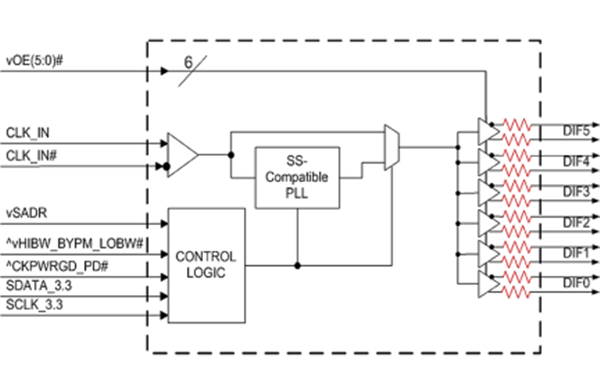
The 9DBU0641AKILF is an ultra-low power PCI Express® buffer from [Renesas], which runs at 1.5V and achieves the lowest power consumption of a PCIe clock device in the industry. The following are its main features and advantages:
Directly connect to 100 transmission lines; Compared with the standard HCSL output, 24 resistors have been saved
The typical power consumption in PLL mode is 46mW, eliminating heat concerns
The output can be powered by any voltage ranging from 1.05 to 1.5V. Maximize energy conservation
Spread spectrum (SS) compatibility; Allow SS to reduce EMI
OE# pin; Support DIF power management
Differential input compatible with HCSL; It can be driven by a public clock source
Optional features of SMBus; Optimize the signal integrity of the application
The slew rate of each output
Differential output amplitude
Pin /SMBus offers optional PLL bandwidth and PLL bypass. Optimize PLL for applications
The output is blocked before the PLL is locked. The cleaning system starts.
The device includes default configurations. The equipment control does not require an SMBus interface
3.3V compatible with SMBus interface supports traditional controllers
Three optional SMBus addresses; Multiple devices can easily share one SMBus network segment
The 40-pin 5x5mm VFQFPN saves space with the smallest circuit board space

Explanation
The 9DBU0641AKILF clock buffer is designed to operate at the same supply voltage as popular system-on-chip (SoC) and field-programmable gate arrays (FPGA), enabling designers to use the same power rail and thereby reducing system complexity, actual size, and power consumption. The low power consumption feature reduces heat dissipation and thereby alleviates the heat dissipation requirements.
The 9DBU0641AKILF PCI Express® clock buffer meets the performance requirements of PCIe Generation 1, 2 and 3, enabling the long-life design to be reused for several generations of products. This clock buffer features an integrated output termination, providing Zo=100 for direct connection to 100 transmission lines. The 9DBU0641AKILF also features six output enables for clock management and three optional SMBus addresses.
Recommended application
1.5V PCIe Gen1-2-3 Zero Delay/fan-out buffer (ZDB/FOB)
Output features
6-1-167 MHz low power (LP) HCSL DIF pairs w/Zo=100
Key specifications
DIF jitter during the cycle is less than 50ps
The output skew of DIF is less than 60ps
The DIF phase jitter complies with the PCIe Gen1-2-3 standard
The additive phase jitter in the DIF bypass mode of PCIe Gen3 is less than 300fs rms
At 12k-20MHz, the additive phase jitter in DIF bypass mode is less than 350fs rms
Basic parameters
Product: 9DBU0641AKILF
Type: Clock buffer
PLL: Yes
Main use: PCI Express (PCIe)
Input: HCSL
Output: LP-HCSL
Number of circuits: 1
Ratio - Input: Output: 1:6
Differential - Input: Output: Yes/Yes
Frequency - Maximum value: 167MHz
Voltage - Power supply: 1.425V to 1.575V
Operating temperature: -40°C to 85°C
Installation type: Surface mount type
Package/Housing: 40-VFQFN
Contact Mingjiada (www.hkmjd.com) immediately for a quote on the 9DBU0641AKILF clock buffer.
![Recycle Microcontroller MCU, Recycle [GigaDevice] GD32E502 Series Microcontrollers](/upload/202509/01/202509011540143370.jpg)
Time:2025-09-01

Time:2025-09-01

Time:2025-09-01

Time:2025-09-01
Contact Number:86-755-83294757
Enterprise QQ:1668527835/ 2850151598/ 2850151584/ 2850151585
Business Hours:9:00-18:00
E-mail:sales@hkmjd.com
Company Address:Room1239, Guoli building, Zhenzhong Road, Futian District, Shenzhen, Guangdong
CopyRight ©2022 Copyright belongs to Mingjiada Yue ICP Bei No. 05062024-12

Official QR Code
Links: