Welcome Here Shenzhen Mingjiada Electronics Co., Ltd.

sales@hkmjd.com

sales@hkmjd.com

Service Telephone:86-755-83294757
 Latest Information
The 8P34S1208NBGI8 is a 2:8 low-voltage differential signal (LVDS) clock buffer launched by Renesas, mainly applied in high-precision clock signal distribution scenarios. The following are the main features of the 8P34S1208NBGI8:• 8 pairs of low skew…
The 8P34S1208NBGI8 is a 2:8 low-voltage differential signal (LVDS) clock buffer launched by Renesas, mainly applied in high-precision clock signal distribution scenarios. The following are the main features of the 8P34S1208NBGI8:
• 8 pairs of low skew and low additional jitter LVDS output
Two optional differential clock input pairs
The differential CLK and nCLK pairs can accept the following differential input levels: LVDS, CML
• Maximum input clock frequency: 1.5GHz
• Control the LVCMOS/LVTTL interface level of the input selection pin
• Output offset: 20ps (typical value)
• Propagation delay: 400ps (maximum)
The 1PPS application has a small variation in propagation delay throughout the entire temperature range
• Low additive phase jitter RMS; fREF = 156.25MHz, VPP = 1V, 12kHz - 20MHz: 34fs (typical value)
• Equipment current Consumption (IDD) :
Typical value of 120mA: 1.8V
Typical value of 132mA: 2.5V
• Full 1.8V or 2.5V power supply voltage
Lead-free (RoHS 6), 28-pin VFQFPN package
Ambient operating temperature: -40°C to 85°C
Supports a housing temperature of up to 105°C
• Supports PCI Express Gen1-5

Overview
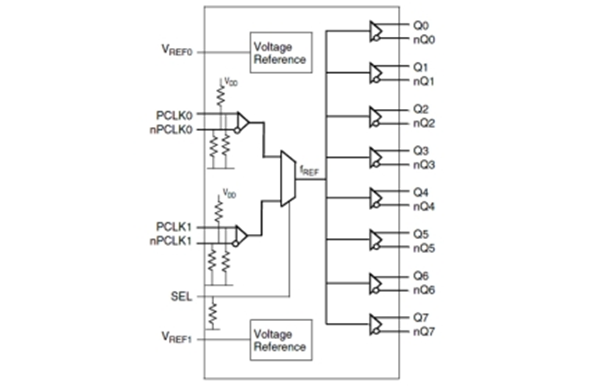
The 8P34S1208NBGI8 is a high-performance differential LVDS fan-out buffer. This device is designed for fan-out 1PPS signals or high-frequency, extremely low additive phase noise clock and data signals. The 8P34S1208NBGI8 supports fail-safe operation and is powered by 1.8V or 2.5V. The guaranteed output-to-output and device-to-device offset characteristics make the 8P34S1208NBGI8 highly suitable for clock distribution applications where performance and repeatability need to be clearly defined. It provides 2 optional differential inputs and 8 low skew outputs. The integrated bias voltage reference enables an easy interface between single-ended signals and differential device inputs. The 8P34S1208NBGI8 has been optimized for low power consumption and low additive phase noise.
Typical applications
The 8P34S1208NBGI8 is suitable for scenarios that require low phase noise and highly stable clock signals, such as:
Communication equipment
Industrial control system
High-precision instruments and meters
Basic information
Product: 8P34S1208NBGI8
Type: Fan-out buffer (allocation), multiplexer
Number of circuits: 1
Ratio - Input: Output: 2:8
Differential - Input: Output: Yes/Yes
Input: CML, LVDS
Output: LVDS
Frequency - Maximum: 1.2 GHz
Voltage - Power supply: 1.71V to 1.89V
Operating temperature: -40°C to 85°C
Installation type: Surface mount type
Packaging/Housing: 28-WFQFN
Welcome to visit the official website of mingjiada (www.hkmjd.com) for exclusive quotations of 8P34S1208NBGI8 clock buffer!
![[In Stock] Supply AM26LV32EIPWR (TI) Quadruple Differential Line Receiver](/upload/202508/26/202508261500001884.jpg)
Time:2025-08-26

Time:2025-08-26

Time:2025-08-26
![Supply [Onsemi] MOSFETs, Mingjiada Supply Power MOSFET, Silicon Carbide (SiC) MOSFET](/upload/202508/26/202508261411186598.jpg)
Time:2025-08-26
Contact Number:86-755-83294757
Enterprise QQ:1668527835/ 2850151598/ 2850151584/ 2850151585
Business Hours:9:00-18:00
E-mail:sales@hkmjd.com
Company Address:Room1239, Guoli building, Zhenzhong Road, Futian District, Shenzhen, Guangdong
CopyRight ©2022 Copyright belongs to Mingjiada Yue ICP Bei No. 05062024-12

Official QR Code
Links: