Welcome Here Shenzhen Mingjiada Electronics Co., Ltd.

sales@hkmjd.com

sales@hkmjd.com

Service Telephone:86-755-83294757
 Latest Information
 Home
/Company Dynamics
/
[Supply-Demand TI] ADC07D1520CIYB: Low Power, 7-Bit, Dual 1.5G SPS Analog-to-Digital Converter (ADC)
The ADC07D1520CIYB is a dual-channel, low-power, high-performance CMOS analog-to-digital converter. Its main features include● 1.9V 0.1V single cropping● Interlaced mode with a 2x sampling rate● Multi-ADC synchronization capabilityAdjust the input …
The ADC07D1520CIYB is a dual-channel, low-power, high-performance CMOS analog-to-digital converter. Its main features include
● 1.9V ±0.1V single cropping
● Interlaced mode with a 2x sampling rate
● Multi-ADC synchronization capability
Adjust the input full-scale range, clock phase and offset
The output clock can be selected as either SDR or DDR
Output demultiplexers of 1:1 or 1:2 are available as options
● The second DCLK output
● Duty cycle correction sampling clock
● Test mode
Overview
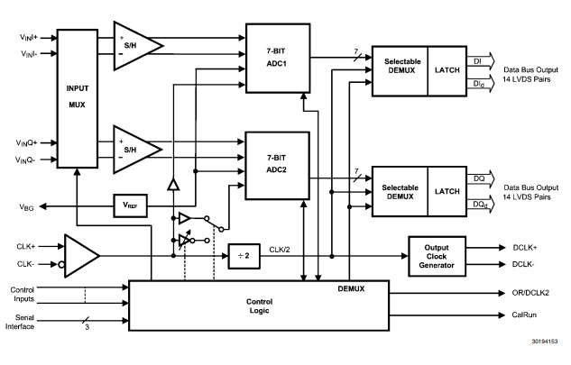
The ADC07D1520CIYB is a dual-channel, low-power, high-performance CMOS analog-to-digital converter. The ADC07D1520CIYB digitizes signals into 7-bit resolution at a sampling rate as high as 1.5 GSPS. Its functions include test mode output for system debugging, clock phase adjustment and an optional output demultiplexer mode. This device ensures that there are no missed codes throughout the entire operating temperature range. The unique folding and interpolation architecture, the fully differential comparator design, the innovative design of the internal sampling-holding amplifier, and the self-calibration scheme make the response of all dynamic parameters very flat, with an input signal of 748 MHz and a sampling rate of 1.5 GHz. Meanwhile, it provides a bit error rate (C.E.R.) of 10-18. The output format is offset binary. The low-voltage differential signal (LVDS) digital output is compatible with IEEE 1596.3-1996, except for the adjustable common-mode voltage between 0.8V and 1.2V.
The ADC07D1520CIYB includes an optional output demultiplexer for feeding two LVDS buses. If the 1:2 Demultiplexed Mode is selected, the output data rate on each bus will be reduced to half of the input sampling rate. When the Non-Demultiplexed Mode is selected, the output data rate on the channel DI and DQ is the same as the rate of the input sampling clock. These two converters can be used alternately and as a single 3 GSPS ADC.
The ADC07D1520CIYB typically consumes less than 3.5mW in power-saving mode. It is available in leaded or lead-free, 128-pin, heat-enhanced exposed pad LQFP packages and can operate within an industrial temperature range (-40 °C ≤ TA ≤ 85°C).

Application scenarios
The ADC07D1520CIYB is suitable for a variety of application scenarios that require high sampling rates and low power consumption, including
● Direct radio frequency down-conversion
● Digital oscilloscope
Satellite set-top box
● Communication system
● Testing instruments
Basic information
Product: ADC07D1520CIYB
Digit number: 7
Sampling rate (per second) : 3G
Input number: 2
Input type: Differential
Data interface: LVDS - Parallel
Configuration: MUX-S/H-ADC
Ratio -S /H:ADC: 1:1
Number of A/D converters: 2
Architecture: Folding and interpolation
Reference type: Internal
Voltage - Power supply, simulation: 1.8V to 2V
Voltage - Power supply, digital: 1.8V to 2V
Feature: Synchronous sampling
Operating temperature: -40°C to 85°C
Package/Shell: 128-HLQFP
Welcome to contact Mingjiada (www.hkmjd.com), get the exclusive quotation of ADC07D1520CIYB products!

Time:2025-09-09

Time:2025-09-09

Time:2025-09-09

Time:2025-09-09
Contact Number:86-755-83294757
Enterprise QQ:1668527835/ 2850151598/ 2850151584/ 2850151585
Business Hours:9:00-18:00
E-mail:sales@hkmjd.com
Company Address:Room1239, Guoli building, Zhenzhong Road, Futian District, Shenzhen, Guangdong
CopyRight ©2022 Copyright belongs to Mingjiada Yue ICP Bei No. 05062024-12

Official QR Code
Links: