Welcome Here Shenzhen Mingjiada Electronics Co., Ltd.

sales@hkmjd.com

sales@hkmjd.com

Service Telephone:86-755-83294757
 Latest Information
 Home
/Company Dynamics
/
(TI New) LMK3C0105V33RERR: 5-Output Reference-Free Clock Generator with (BAW) Technology
The LMK3C0105V33RERR is a reference-free clock generator with five output ports using bulk Acoustic wave (BAW) technology . This device does not require an external reference and can provide a stable clock output, making it suitable for a variety of…
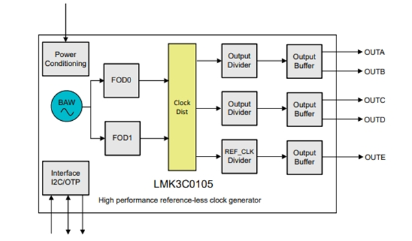
The LMK3C0105V33RERR is a reference-free clock generator with five output ports using bulk Acoustic wave (BAW) technology . This device does not require an external reference and can provide a stable clock output, making it suitable for a variety of application scenarios.

Its main features include
Integrated BAW resonator, no external reference required
Flexible frequency generation
100MHz to 400MHz dual-channel fractional output crossover (FOD)
Two-channel crossover: Up to three unique output frequencies, ranging from 2.5MHz to 200MHz
Example: OUTA/B/C/D/E = 25MHz
OUTA/B = 100MHz, OUTC/D =50MHz, OUTE = 25MHz
Supported 1.8V/2.5V/3.3V LVCMOS output, up to 200MHz at most
Generate up to 5 LVCMOS clocks on the OUTA to OUTE pins
±25ppm total output frequency stability
Two operation modes: I2C or pre-programmed OTP
Ambient temperature: -40 °C to 85°C.
Support for hybrid SSC and non-SSC output
Programmable SSC modulation depth
Pre-programming: Downward spread spectrum of -0.1%, -0.25%, -0.3% and -0.5%
Register programmable: -0.1% to -3% downward spread frequency or ±0.05% to ±1.5% center spread frequency
VDD = VDDO = 1.8V/2.5V/3.3V ± 5%
The startup time is less than 5ms
When the output comes from the same FOD, the output-to-output offset is less than 50ps
Failure protection input and VDD pins
Description
The LMK3C0105V33RERR is a 5-output no-reference clock generator with SSC support. The LMK3C0105V33RERR is based on TI's proprietary bulk acoustic wave (BAW) technology and can provide ±25ppm clock output without any crystal or external clock reference. The LMK3C0105V33RERR can simultaneously provide 5 SSC clocks, 5 non-SSC clocks, or a combination of SSC and non-SSC clocks. Five outputs can generate up to three different output frequencies. Each output channel can select any FOD as the frequency source to generate four LVCMOS clocks. The REF_CTRL pin is used as the fifth LVCMOS clock output, and any FOD can be selected as the source.
This device can be easily configured through GPIO pins or the I2C interface. The LMK3C0105V33RERR has an excellent PSNR and does not require any external LDO.
Basic parameters
Product: LMK3C0105V33RERR
Type: Clock Generator
PLL: None
Input: -
Output: LVCMOS
Number of circuits: 1
Ratio - Input: Output: 0:5
Differential - Input: Output: None/None
Frequency - Maximum value: 200MHz
Frequency divider/frequency multiplier: None/Yes
Voltage - Power supply: 1.71V - 1.89V, 2.375V - 2.625V, 3.135V - 3.465V
Operating temperature: -40°C to 85°C (TA)
Installation type: Surface mount type
Package/Shell: 16-TFQFN
Application field
LMK3C0105V33RERR is widely applied in the following fields:
Alternative crystal : As a clock source alternative to conventional crystals for applications that require multiple clock outputs.
ASIC, FPGA, MCU : PROVIDE a stable reference clock for these chips.
Industrial communications : Provide a stable clock signal in industrial communications systems.
Industrial PC and Human-Machine interface (HMI) : Ensure system synchronization and stable operation.
Wired network : provides stable clock support in data transmission and communication.
Act now: Visit www.hkmjd.com or call +86 13410018555 for a quote on LMK3C0105V33RERR!

Time:2025-09-09

Time:2025-09-09

Time:2025-09-09

Time:2025-09-09
Contact Number:86-755-83294757
Enterprise QQ:1668527835/ 2850151598/ 2850151584/ 2850151585
Business Hours:9:00-18:00
E-mail:sales@hkmjd.com
Company Address:Room1239, Guoli building, Zhenzhong Road, Futian District, Shenzhen, Guangdong
CopyRight ©2022 Copyright belongs to Mingjiada Yue ICP Bei No. 05062024-12

Official QR Code
Links: