Welcome Here Shenzhen Mingjiada Electronics Co., Ltd.

sales@hkmjd.com

sales@hkmjd.com

Service Telephone:86-755-83294757
 Latest Information
 Home
/Company Dynamics
/
ADI High Speed a/D Converter: LTC2141CUP-12 12-Bit, 40 Msps, Low Power, Dual ADC
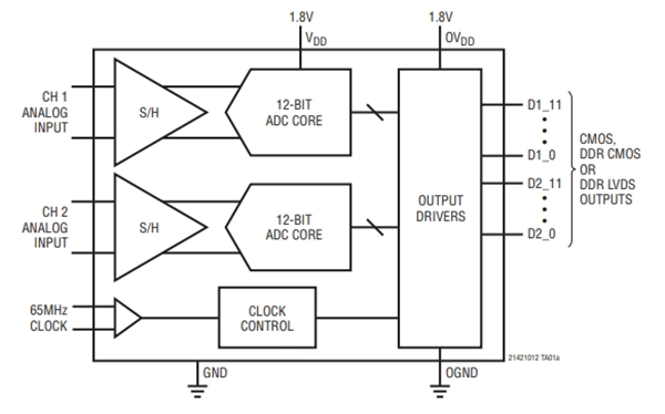
LTC2141CUP-12:12-bit, 40Msps, low-power, dual-channel analog-to-digital converterMain characteristicsTwo-channel simultaneous sampling ADC70.8dB SNR89dB SFDRLow power: 92mW / 65mW / 48mW (total value)46mW / 33mW / 24mW (per channel)Single 1.8V power s…
LTC2141CUP-12:12-bit, 40Msps, low-power, dual-channel analog-to-digital converter

Main characteristics
Two-channel simultaneous sampling ADC
70.8dB SNR
89dB SFDR
Low power: 92mW / 65mW / 48mW (total value)
46mW / 33mW / 24mW (per channel)
Single 1.8V power supply
CMOS, DDR CMOS, or DDR LVDS output
Optional input range: 1VP-P to 2VP-P
750MHz full-power bandwidth sampling and holding (S/H)
Optional random function generator for data output
Optional clock duty cycle stabilizer
Sleep and nap patterns
Serial SPI port for configuration
Pin (9mm x 9mm) QFN package
Description
The LTC2141CUP-12 is A dual-channel simultaneous sampling 12-bit A/D converter, specifically designed for digital processing of high-frequency and wide dynamic range signals. The LTC2141CUP-12 device is highly suitable for demanding communication applications. Its AC performance includes 70.8dB SNR and 89dB parasitic dynamic range (SFDR). The ultra-low jitter of 0.08psRMS achieves undersampling at the IF frequency and excellent noise performance.
The DC specification includes ±0.3LSB INL (typical value), ±0.1LSB DNL (typical value) and no missed codes throughout the entire temperature range. The LTC2141CUP-12 converts noise to 0.3LSBRMS.
The digital output of LTC2141CUP-12 can be full-rate CMOS, double data rate CMOS or double data rate LVDS. A separate output power supply provides a CMOS output swing ranging from 1.2V to 1.8V.
The LTC2141CUP-12 can perform differential or single-ended driving of ENC+ and ENC- inputs using a sine wave, PECL, LVDS, TTL or CMOS input. An optional clock duty cycle stabilizer achieves high performance under full-speed and multiple clock duty cycle conditions.
The LTC2141CUP-12 has the following key parameters:
Digit number: 12
Sampling rate (per second) : 40M
Input number: 2
Input type: Differential
Data interface: LVDS - Parallel, Parallel
Configuration: S/H-ADC
Ratio -S /H:ADC: 1:1
Number of A/D converters: 2
Architecture: Pipeline
Reference types: External, Internal
Voltage - Power supply, simulation: 1.7V to 1.9V
Voltage - Power supply, digital: 1.7V to 1.9V
Feature: Synchronous sampling
Operating temperature: 0°C to 70°C
Package/Shell: 64-WFQFN
Application scenario
The LTC2141CUP-12 is highly suitable for demanding communication applications, such as wireless infrastructure, test and measurement equipment, and high-speed data acquisition systems, etc. Its high performance and low power consumption make it excel in these applications .
Our website: www.hkmjd.com

Time:2025-09-09

Time:2025-09-09

Time:2025-09-09

Time:2025-09-09
Contact Number:86-755-83294757
Enterprise QQ:1668527835/ 2850151598/ 2850151584/ 2850151585
Business Hours:9:00-18:00
E-mail:sales@hkmjd.com
Company Address:Room1239, Guoli building, Zhenzhong Road, Futian District, Shenzhen, Guangdong
CopyRight ©2022 Copyright belongs to Mingjiada Yue ICP Bei No. 05062024-12

Official QR Code
Links: