Welcome Here Shenzhen Mingjiada Electronics Co., Ltd.

sales@hkmjd.com

sales@hkmjd.com

Service Telephone:86-755-83294757
 Latest Information
 Home
/Company Dynamics
/
Analog Devices Clock Buffer | HMC7043LP7FE: High Performance, 3.2 GHz, 14 Output Fanout Buffer
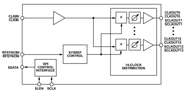
Analog Devices Inc. HMC7043LP7FE: A high-performance, 3.2GHz, 14-output fend-out bufferIts main characteristicsSupport JEDEC JESD204BLow-additive jitter: <15 fs rms (2457.6 MHz, 12 kHz to 20 MHz)Extremely low noise: -155.2 dBc/Hz (983.04 MHz)Up to …
Analog Devices Inc. HMC7043LP7FE: A high-performance, 3.2GHz, 14-output fend-out buffer
Its main characteristics
Support JEDEC JESD204B
Low-additive jitter: <15 fs rms (2457.6 MHz, 12 kHz to 20 MHz)
Extremely low noise: -155.2 dBc/Hz (983.04 MHz)
Up to 14 channels of LVDS, LVPECL or CML-type device clocks (DCLK) are provided.
The maximum frequency of CLKOUTx/CLKOUTx and SCLKOUTx/SCLKOUTx reaches 3200 MHz
JESD204B compatible System Reference (SYSREF) pulse
25 ps analog delay and ½ clock input cycle digital delay, each of the 14 clock output channels can be programmed for delay
The relationship between the adjustable noise base and power consumption can be programmed through SPI
SYSREF valid interrupts can simplify JESD204B synchronization
Support deterministic synchronization of multiple HMC7043 devices
The RFSYNC pin or SpI-controlled SYNC trigger is used to output the synchronous JESD204B
GPIO alarm/status indication is used to determine the system status
The clock input supports frequencies up to 6 GHz
The on-chip regulator provides excellent PSRR
48-pin, 7mm × 7mm LFCSP package

Overview
The HMC7043LP7FE is designed to meet the requirements of multi-carrier GSM and LTE base station design and simplify the design of baseband and radio card clock trees through multiple clock management and allocation features.
The HMC7043LP7FE offers 14 channels of low-noise and configurable outputs, which can be flexibly interface with many different devices in the base station transceiver (BTS) system, such as data converters, local oscillators, transmit/receive modules, field programmable gate arrays (FPgas), and digital front-end ASics, etc. The HMC7043LP7FE can generate up to 7 DCLK and SYSREF clock pairs that comply with the JESD204B interface requirements.
System designers can generate fewer DCLK and SYSREF pairs and configure the remaining output signal paths for independent phases and frequencies. Both the DCLK and SYSREF clock outputs can be configured to support different signal standards such as CML, LVDS, LVPECL, and LVCMOS. Different bias conditions can adjust the changing board insertion loss.
One of the unique features of the HMC7043LP7FE is its independent and flexible phase management for each of the 14 channels. All 14 channels support frequency and phase adjustment. These outputs can also be programmed for internal and external termination options of 50 Ω or 100 Ω.
The HMC7043LP7FE device has the RF SYNC function and supports deterministic synchronization of multiple HMC7043 devices, that is, ensuring that all clock outputs start from the same clock edge. This can be achieved by rewriting the nested HMC7043LP7FE or SYSREF control unit/divider and then restarting the output divider with a new phase.
The HMC7043LP7FE is available in a 48-pin, 7mm × 7mm LFCSP package with exposed pads grounded.
The HMC7043LP7FE has the following key parameters:
PLL: Yes
Input: Clock
Output: CML, LVDS, LVPECL
Number of circuits: 1
Ratio - Input: Output: 1:14
Differential - Input: Output: Yes/Yes
Frequency - Maximum: 3.2GHz
Frequency divider/frequency multiplier: Yes/No
Voltage - Power supply: 3.135V to 3.465V
Operating temperature: -40°C to 85°C
Installation type: Surface mount type
Package/Shell: 48-LFCSP
In addition, the HMC7043LP7FE clock buffer is widely used in various application scenarios, mainly including:
The JESD204B clock is generated
Cellular infrastructure (multi-carrier GSM, LTE, W-CDMA)
Data converter clock
Phased array reference allocation
Microwave baseband card
For the purchase of HMC7043LP7FE clock buffer, please visit www.hkmjd.com for more details.

Time:2025-09-09

Time:2025-09-09

Time:2025-09-09

Time:2025-09-09
Contact Number:86-755-83294757
Enterprise QQ:1668527835/ 2850151598/ 2850151584/ 2850151585
Business Hours:9:00-18:00
E-mail:sales@hkmjd.com
Company Address:Room1239, Guoli building, Zhenzhong Road, Futian District, Shenzhen, Guangdong
CopyRight ©2022 Copyright belongs to Mingjiada Yue ICP Bei No. 05062024-12

Official QR Code
Links: