Welcome Here Shenzhen Mingjiada Electronics Co., Ltd.

sales@hkmjd.com

sales@hkmjd.com

Service Telephone:86-755-83294757
 Latest Information
 Home
/Company Dynamics
/
ADI LTC2185Iup Analog-to-Digital Converter: 16-Bit, 125Msps, Low Power, Dual ADC
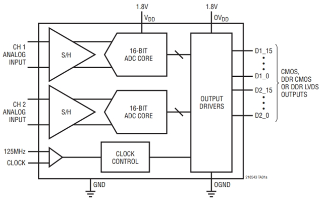
The LTC2185IUP standard high speed analog-to-digital converter is a 16-bit, 125Msps, low power, dual-channel ADC designed specifically for the digital processing of high frequency, wide dynamic range signals .Key FeaturesThe main features of LTC2185…
The LTC2185IUP standard high speed analog-to-digital converter is a 16-bit, 125Msps, low power, dual-channel ADC designed specifically for the digital processing of high frequency, wide dynamic range signals .

Key Features
The main features of LTC2185IUP include:
Two-channel simultaneous sampling ADC
76.8dB SNR
90dB SFDR
Low power: 370mW / 308mW / 200mW (total)
185mW / 154mW / 100mW (per channel)
Single 1.8V power supply
CMOS, DDR CMOS or DDR LVDS output
Optional input range: 1VP-P to 2VP-P
550MHz full power bandwidth S/H (sampling and holding)
Optional data output random function generator
Optional clock duty cycle stabilizer
Shutdown and nap mode
Serial SPI port for configuration
64-pin (9mm x 9mm) QFN package
Product Details
The LTC2185IUP is A two-channel simultaneous sampling 16-bit A/D converter, specifically designed for digital processing of high-frequency and wide dynamic range signals. The LTC2185IUP is highly suitable for demanding communication applications, with its AC performance including 76.8dB SNR and 90dB parasitic dynamic range (SFDR). The ultra-low jitter of 0.07psRMS achieves undersampling at the IF frequency and excellent noise performance.
The DC specification includes ±2LSB INL (typical value), ±0.5LSB DNL (typical value) and no missed codes throughout the entire temperature range. Convert the noise to 3.4LSBRMS.
The digital output can be full-rate CMOS, double data rate CMOS or double data rate LVDS. A separate output power supply provides a CMOS output swing ranging from 1.2V to 1.8V.
Differential or single-ended driving of ENC+ and ENC - inputs can be performed using a sine wave, PECL, LVDS, TTL or CMOS input. An optional clock duty cycle stabilizer achieves high performance under full-speed and multiple clock duty cycle conditions.
Application field
The LTC2185IUP is applicable to the following fields:
Communication
Cellular base station
Software-defined radio
Portable medical imaging
Multi-channel data acquisition
Non-destructive testing
Performance parameters
Model: LTC2185IUP
Resolution: 16 bits
Number of channels: 2 channels
Sampling ratio: 125 MS/s
Input type: Differential/Single-Ended
Structure: Pipeline
Analog power supply voltage: 1.8V
Package/Box: QFN-64
Development kits: DC1620A-A, DC1945A
DNL - Differential nonlinearity: 0.5 LSB
Inl-integral nonlinearity: 2 LSB
Pd- Power dissipation: 370 mW
Product type: ADCs-Analog to Digital Converters
Reference type: Internal
SFDR - Stray dynamic range: 90 dB
Shutdown
SINAD - Signal-to-noise and distortion rate: 76.6 dB
【 Consult now 】
For real-time inventory status of LTC2185IUP, please contact Mingjiada Electronics directly at (www.hkmjd.com).
![Supply [ADI] LDO Linear Regulators, LED Driver IC, Battery Management IC](/upload/202507/21/202507211436467273.jpg)
Time:2025-07-21

Time:2025-07-21

Time:2025-07-21

Time:2025-07-21
Contact Number:86-755-83294757
Enterprise QQ:1668527835/ 2850151598/ 2850151584/ 2850151585
Business Hours:9:00-18:00
E-mail:sales@hkmjd.com
Company Address:Room1239, Guoli building, Zhenzhong Road, Futian District, Shenzhen, Guangdong
CopyRight ©2022 Copyright belongs to Mingjiada Yue ICP Bei No. 05062024-12

Official QR Code
Links: