Welcome Here Shenzhen Mingjiada Electronics Co., Ltd.

sales@hkmjd.com

sales@hkmjd.com

Service Telephone:86-755-83294757
 Latest Information
 Home
/Company Dynamics
/
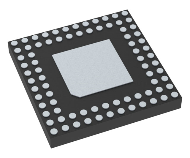
Microchip A2F200M3F-1CS288I SmartFusion System-on-Chip (SoC)FPGA product Overview
Product Overview:The A2F200M3F-1CS288I SmartFusion system-on-Chip (SoC)FPGA is the only device that integrates an FPGA architecture, Arm Cortex-M3 processor, and programmable analog circuitry, providing the benefits of full customization and ip protec…
Product Overview:
The A2F200M3F-1CS288I SmartFusion system-on-Chip (SoC)FPGA is the only device that integrates an FPGA architecture, Arm Cortex-M3 processor, and programmable analog circuitry, providing the benefits of full customization and ip protection while still being easy to use.
Based on a proprietary flash memory process, SmartFusion SoC FPgas are ideal for hardware and embedded designers who need a true SoC solution that offers greater flexibility than traditional fixed-function microcontrollers without the exorbitant cost of soft processor cores on traditional FPgas.

Features:
Microcontroller System (MSS) :
The 100 MHz 32-bit ARM® Cortex™-M3, zero-wait state memory achieves 1.25 DMIPS/MHz throughput
Memory Protection Unit (MPU)
Single cycle multiplication, hardware division
JTAG debugging (four-wire), Serial line debugging (SWD - two-wire) and single-wire browser (SWV) interfaces
Embedded Flash memory (eNVM), 64K to 512K bytes
Embedded high-speed SRAM (eSRAM), 16K bytes ~ 64K bytes, including 2 physical blocks, 2 different hosts can access it at the same time
On-chip memory bandwidth up to 16 Gbps
10/100 Ethernet MAC with RMII interface
Programmable external memory controller
Asynchronous memory
NOR Flash, SRAM, PSRAM
Synchronous SRAM
Two I2C peripherals
Two 16550 UART
Two SPI peripherals
Two 32-bit timers
32-bit watchdog timer
8-channel DMA controller
1.5MHz ~ 20MHz master oscillator
Battery-operated 32 KHz low power oscillator with real-time counter (RTC)
100 MHz embedded RC oscillator with 1% accuracy
Embedded PLL with 4 output phases
High performance FPGA:
A Flash-based, 130nm, 7-layer metal CMOS process is used
Non-volatile, retain program in case of power failure
350 MHz system performance
Embedded SRAM with FIFO
The aspect ratio of the SRAM block is adjustable
The combination of ×1, ×2, ×4, ×9 and ×18 can be selected
True dual-port SRAM (except ×18 combinations)
Programmable embedded FIFO control logic
Secure ISP with 128-bit Advanced Encryption Standard (AES) decryption technology through JTAG
The FPGA content is protected by FlashLock technology
Five clock Regulating circuit (CCC) modules with up to two integrated analog PLLS per module
Phase shift, frequency division/doubling, delay, etc. can be configured
Frequency: Input is 1.5 ~ 350 MHz, output is 0.75 ~ 350 MHz
Programmable Analog Front End (AFE) :
Up to three 12-bit SAR ADCs can be included
The rate is 500 Ksps in 12-bit mode
The rate is 600 Ksps in 8-bit and 10-bit modes
2.56V Internal or external reference voltage
Each ADC contains a first-level Sigma-Delta (Σ-) DAC
12-bit 500 Ksps update rate
Each device can contain up to five new high-performance analog signal conditioning modules (SCBS), each consisting of:
2 high-voltage bipolar voltage monitors (±2.5V to -11.5/+14V for 4 inputs) with 1% accuracy
High gain current monitor, differential gain =50, common-mode voltage up to 14V
Temperature monitor (resolution =1/4℃ in 12-bit mode; The accurate temperature range is -55℃ ~ 150℃)
Up to 10 high-speed comparators (tpd = 50ns)

Time:2025-07-08

Time:2025-07-08

Time:2025-07-08
![Mingjiada Electronics One-stop Supply [ST] Full Range of Motor Driver ICs](/upload/202507/08/202507080956504363.jpg)
Time:2025-07-08
Contact Number:86-755-83294757
Enterprise QQ:1668527835/ 2850151598/ 2850151584/ 2850151585
Business Hours:9:00-18:00
E-mail:sales@hkmjd.com
Company Address:Room1239, Guoli building, Zhenzhong Road, Futian District, Shenzhen, Guangdong
CopyRight ©2022 Copyright belongs to Mingjiada Yue ICP Bei No. 05062024-12

Official QR Code
Links: