Welcome Here Shenzhen Mingjiada Electronics Co., Ltd.

sales@hkmjd.com

sales@hkmjd.com

Service Telephone:86-755-83294757
 Latest Information
 Home
/Company Dynamics
/
8T49N283C-999NLGI: A FemtoClock NG dual-channel universal frequency synthesizer
The 8T49N283C-999NLGI is a clock generator/frequency synthesizer /PLL chip released by [Renesas]. It is packaged in VFQFPN-56 and supports surface mount. The following are its core features:Supports SDH/SONET and synchronous Ethernet clocks, including…
The 8T49N283C-999NLGI is a clock generator/frequency synthesizer /PLL chip released by [Renesas]. It is packaged in VFQFPN-56 and supports surface mount. The following are its core features:
Supports SDH/SONET and synchronous Ethernet clocks, including all FEC rate conversions
The two differential outputs meet the jitter limits of 100G Ethernet and STM-256/OC-768
• <0.3ps RMS (including spurious) : 12kHz to 20MHz
All outputs <0.5ps RMS (including spurious) from 12kHz to 20MHz
• Operation mode: Lock the input signal, hold and run freely
The initial holding accuracy is ±50ppb
• Accepts up to two LVPECL, LVDS, LVHSTL or LVCMOS input clocks
It accepts frequencies ranging from 8kHz to 875MHz
• Automatic and manual input clock selection, with uninterrupted switching
• Clock input monitoring, including support for intermittent clocks
Phase slope limit and complete uninterrupted switching option for controlling output phase transients
• Crystal oscillator operating in base frequency mode from 10MHz to 40MHz
Generate 8 LVPECL/LVDS or 16 LVCMOS output clocks
The output frequency range is from 8kHz to 1.0GHz (diff)
The output frequency range is from 8kHz to 250MHz (LVCMOS)
• Four universal I/O pins, optional support for status and control:
Four output enable control inputs can be mapped to any one of the eight outputs
• Lock, hold and signal loss status output
• Open the leak interrupt pin
• Programmable PLL bandwidth Settings for each PLL
0.5Hz, 1Hz, 2Hz, 4Hz, 8Hz, 16Hz, 32Hz, 64Hz, 128Hz, 256Hz or 512Hz
Optional quick lock function
• Programmable output phase delay, with a step size as low as 16ps
Register programming is performed via I2C or an external I2C EEPROM
• Bypass clock path for system testing
• Power supply mode
VCC / VCCA / VCCO
3.3V / 3.3V / 3.3V
3.3V / 3.3V / 2.5V
3.3V / 3.3V / 1.8V (low-voltage coupling)
2.5V / 2.5V / 3.3V
2.5V / 2.5V / 2.5V
2.5V / 2.5V / 1.8V (Low frequency)
The power-saving mode supports power consumption as low as 1.7W (for detailed information, please refer to Power Dissipation and Heat Dissipation Notes).
Ambient operating temperature: -40°C to 85°C
• Package: 56QFN, lead-free (RoHS 6)

Overview
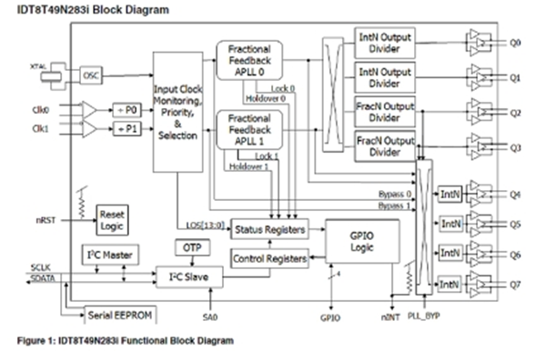
The 8T49N283C-999NLGI is a device with two independent fractional feedback PLLS that can be used as a jitter attenuator and frequency converter. The 8T49N283C-999NLGI is equipped with a 6-integer and 2-decimal output divider, allowing for the generation of up to 8 different output frequencies, ranging from 8kHz to 1GHz. Among them, four frequencies are independent of each other and completely independent of inputs. The other four are related frequencies. The 8-channel output can be selected among LVPECL, LVDS or LVCMOS output levels.
This makes it highly suitable for any frequency conversion application, including 1G, 10G, 40G and 100G synchronous Ethernet, OTN and SONET/SDH, including ITU-T G.709 (2009) FEC rates. The 8T49N283C-999NLGI can also serve as a frequency synthesizer.
The 8T49N283C-999NLGI can accept up to two differential or single-ended input clocks and one crystal oscillator input. Both internal PLLS can lock different input clocks, which may have independent frequencies. Each PLL can use another input as a redundant backup of the master clock, but in this case, the frequencies of the two input clocks must be related.
The 8T49N283C-999NLGI supports uninterrupted reference switching between input clocks. The 8T49N283C-999NLGI monitors signal loss (LOS) of all input clocks and generates an alarm when an input clock failure is detected. Support automatic and manual uninterrupted reference switching options. The LOS behavior can be set to support gap-free or gap-free clocks.
In addition, the 8T49N283C-999NLGI also supports the retention of each PLL. The initial accuracy maintained from the time when all available input reference voltage sources are detected to be lost is 50ppB. It maintains a historical average operating point for each PLL, and in hold mode, this point may return with a limited phase slope.
Typical applications
OTN or SONET/SDH equipment line card (up to OC-192, and supports FEC ratio)
OTN decommapping (Gap clock and DCO mode)
Gigabit and terbit IP switches/routers, including support for synchronous Ethernet
Wireless base station baseband
Data communication
In addition, the core parameters of 8T49N283C-999NLGI are
PLL: With bypass
Input: Crystal
Output: LVCMOS, LVPECL
Number of circuits: 1
Ratio - Input: Output: 1:8
Differential - Input: Output: None/Yes
Frequency - Maximum: 1GHz
Frequency divider/frequency doubler: Yes/No
Voltage - Power supply: 2.375V to 3.465V
Operating temperature: -40°C to 85°C
Installation type: Surface mount type
Packaging/Housing: 56-VFQFN
For an exclusive quote for the 8T49N283C-999NLGI chip, please contact www.hkmjd.com.
![[In Stock] Supply AM26LV32EIPWR (TI) Quadruple Differential Line Receiver](/upload/202508/26/202508261500001884.jpg)
Time:2025-08-26

Time:2025-08-26

Time:2025-08-26
![Supply [Onsemi] MOSFETs, Mingjiada Supply Power MOSFET, Silicon Carbide (SiC) MOSFET](/upload/202508/26/202508261411186598.jpg)
Time:2025-08-26
Contact Number:86-755-83294757
Enterprise QQ:1668527835/ 2850151598/ 2850151584/ 2850151585
Business Hours:9:00-18:00
E-mail:sales@hkmjd.com
Company Address:Room1239, Guoli building, Zhenzhong Road, Futian District, Shenzhen, Guangdong
CopyRight ©2022 Copyright belongs to Mingjiada Yue ICP Bei No. 05062024-12

Official QR Code
Links: