Welcome Here Shenzhen Mingjiada Electronics Co., Ltd.

sales@hkmjd.com

sales@hkmjd.com

Service Telephone:86-755-83294757
 Latest Information
 Home
/Industry Information
/
SAMSUNG's First QLC Ninth Generation V-NAND for AI Era Starts Mass Production
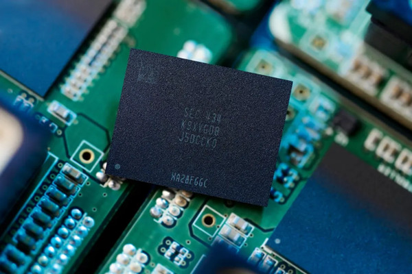
SAMSUNG recently announced that the first 1 terabit (Tb) four-layer unit (QLC) 9th generation V-NAND (V-NAND) has officially begun mass production.In April, SAMSUNG launched its first triple layer unit (TLC) 9th generation V-NAND, followed by the firs…
SAMSUNG recently announced that the first 1 terabit (Tb) four-layer unit (QLC) 9th generation V-NAND (V-NAND) has officially begun mass production.

In April, SAMSUNG launched its first triple layer unit (TLC) 9th generation V-NAND, followed by the first QLC 9th generation V-NAND, further strengthening SAMSUNG's position in the high-capacity, high-performance NAND flash memory market.
SungHoi Hur, executive vice president and Head of Flash Products and Technology at SAMSUNG, said:
The successful launch of QLC 9th Generation V-NAND just four months after the last TLC release, allows us to offer a complete lineup of SSD solutions that meet the demands of the AI era. As the enterprise SSD market shows a growing trend and the demand for AI applications is stronger, we will continue to strengthen SAMSUNG's market position in this segment with QLC and TLC 9th Generation V-NAND."
SAMSUNG plans to expand the range of QLC 9th Generation V-NAND applications, starting with branded consumer products and expanding to mobile Universal Flash memory (UFS), personal computers and server SSDS for customers including cloud service providers.
SAMSUNG QLC 9th generation V-NAND integrates a number of innovations to achieve a number of technological breakthroughs.
• SAMSUNG's proud Channel Hole Etching technology can achieve the highest number of cell layers in the industry based on a dual-stack architecture. SAMSUNG applied the technical experience accumulated in TCL's 9th generation V-NAND to optimize the memory unit area and peripheral circuits, and improved the bit density by about 86% compared to the previous generation QLC V-NAND.
• Designed Mold technology adjusts the word line (WL) spacing of the control storage unit to ensure that the characteristics of the storage unit within and between the same cell layer are consistent for optimal results. The more V-NAND layers there are, the more important the storage unit features are. The use of preset mold technology improves data retention performance by about 20% compared to previous versions, enhancing product reliability.
Predictive Program technology predicts and controls state changes in storage units, minimizing unnecessary operations. This technological advancement doubles the write performance of SAMSUNG QLC 9th Generation V-NAND and increases the data input/output speed by 60%.
• Low-Power Design technology reduces data reading power by approximately 30% and 50%, respectively. This technology reduces the voltage required to drive the NAND storage unit, enabling only the necessary bit lines (BLS) to be sensed, thereby minimizing power consumption.
To learn more, visit news.samsung.com.
Company website: www.hkmjd.com
![Mingjiada Supply [ADI] LT3502AEDC 500mA, Step-Down DC/DC Regulators](/upload/202508/19/202508191511211474.jpg)
Time:2025-08-19

Time:2025-08-19
![[Mingjiada] High-price Acquisition Of IGBT/AI/5G Modules, Recycling Of Infineon/Qualcomm/NVIDIA](/upload/202508/19/202508191410082965.jpg)
Time:2025-08-19
![Supply IC Chips——Supply [TI] MCU, PMIC Chip, ADC/DAC, RF Devices, Sensors](/upload/202508/19/202508191403203123.jpg)
Time:2025-08-19
Contact Number:86-755-83294757
Enterprise QQ:1668527835/ 2850151598/ 2850151584/ 2850151585
Business Hours:9:00-18:00
E-mail:sales@hkmjd.com
Company Address:Room1239, Guoli building, Zhenzhong Road, Futian District, Shenzhen, Guangdong
CopyRight ©2022 Copyright belongs to Mingjiada Yue ICP Bei No. 05062024-12

Official QR Code
Links: