Welcome Here Shenzhen Mingjiada Electronics Co., Ltd.

sales@hkmjd.com

sales@hkmjd.com

Service Telephone:86-755-83294757
 Latest Information
 Home
/Industry Information
/
Samsung Electronics Builds HBM4 Memory Logic Chip on Its Own 4nm Advanced Process
July 16, The Korea Economic News (hankyung) reported yesterday that Samsung Electronics has decided to use its own 4nm process to build the Logic Die in the next generation of HBM memory -- HBM4.Layers of stacked DRAM Die memory chips provide the capa…
July 16, The Korea Economic News (hankyung) reported yesterday that Samsung Electronics has decided to use its own 4nm process to build the Logic Die in the next generation of HBM memory -- HBM4.
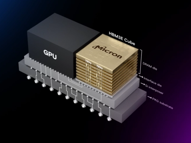
Layers of stacked DRAM Die memory chips provide the capacity for the HBM memory; while the Logic Die is the control unit of the DRAM stack, and is also responsible for communicating with the memory interface on the processor through the interconnect layer, which is also an important part of the HBM memory.
Traditionally, storage vendors have produced the Logic Die for HBM memory using their own storage semiconductor process, which is a much simpler process. However, in the HBM4 generation, Logic Die needs to support more signal pins, larger data bandwidth, and even carry some customized functions.
Therefore, storage vendors choose to cooperate with logic foundries to produce Logic Die for HBM4 with logic semiconductor process.
Previously it was rumored that TSMC will use 7nm process for SK Hynix foundry HBM4 base die.
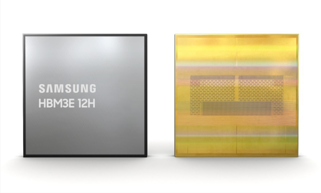
Samsung Electronics' storage division has adopted its own 4nm process to build logic chips, which on one hand can improve the comprehensive energy efficiency of HBM4 memory and enhance product competitiveness; on the other hand, the more delicate 4nm process also leaves more space for the introduction of various customized functions.
On the other hand, the more delicate 4nm process also leaves more room for the introduction of various customized functions. In addition, this move can also provide a sizeable order for the sister unit LSI department.
For Samsung's storage division, the introduction of LSI's advanced process into its products is not unprecedented: its consumer SSD PM9C1a for OEMs is also equipped with LSI's 5nm main control.
![[Supply TI Sensors] LMT87QDCKRQ1——Automotive ±2.7°C Analog Output Temperature Sensor](/upload/202508/20/202508201535497552.jpg)
Time:2025-08-20
Time:2025-08-20
Time:2025-08-20

Time:2025-08-20
Contact Number:86-755-83294757
Enterprise QQ:1668527835/ 2850151598/ 2850151584/ 2850151585
Business Hours:9:00-18:00
E-mail:sales@hkmjd.com
Company Address:Room1239, Guoli building, Zhenzhong Road, Futian District, Shenzhen, Guangdong
CopyRight ©2022 Copyright belongs to Mingjiada Yue ICP Bei No. 05062024-12

Official QR Code
Links: