Welcome Here Shenzhen Mingjiada Electronics Co., Ltd.


sales@hkmjd.com
sales@hkmjd.com


Service Telephone:86-755-83294757
 Latest Information
 Home
/Company Dynamics
/
Home
/Company Dynamics
/
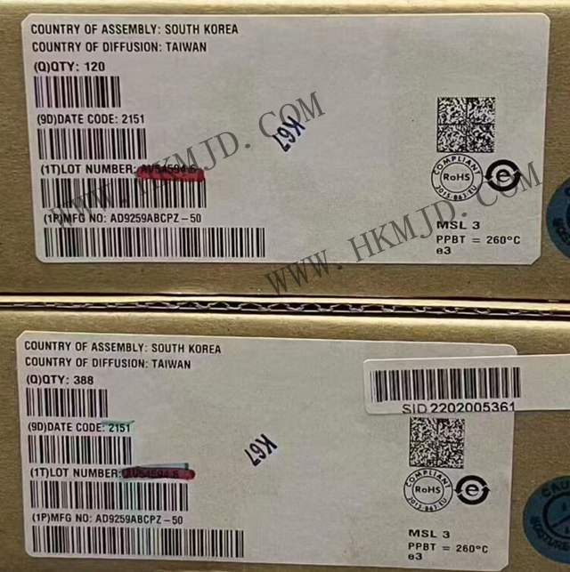
ADI AD9259ABCPZ-50 Quad 14-Bit 50MSPS Serial LVDS 1.8V Analog-to-Digital Converter
ADI AD9259ABCPZ-50 Quad 14-Bit 50MSPS Serial LVDS 1.8V Analog-to-Digital ConverterShenzhen Mingjiada Electronics Co., Ltd., as a leading global distributor of electronic components, has been supplying the ADI high-performance analogue-to-digital conve…
ADI AD9259ABCPZ-50 Quad 14-Bit 50MSPS Serial LVDS 1.8V Analog-to-Digital Converter
Shenzhen Mingjiada Electronics Co., Ltd., as a leading global distributor of electronic components, has been supplying the ADI high-performance analogue-to-digital converter AD9259ABCPZ-50 for an extended period. This four-channel, 14-bit, 50 MSPS serial LVDS 1.8V ADC finds extensive application in fields such as medical imaging, communication systems, and industrial automation.
【Product Overview and Key Features of the AD9259ABCPZ-50】
The AD9259ABCPZ-50 is a four-channel, 14-bit, 50 MSPS analogue-to-digital converter (ADC) with an integrated sample-and-hold circuit, designed for low cost, low power consumption, miniaturisation, and ease of use. The AD9259ABCPZ-50 operates at a maximum conversion rate of 50 MSPS and is optimised for exceptional dynamic performance and low power consumption, making it particularly suitable for applications with strict packaging size requirements.
The AD9259ABCPZ-50 requires only a single 1.8V power supply and supports LVPECL-/CMOS-/LVDS-compatible sampling rate clocks for full-performance operation. Many applications do not require external reference or driver components.
The AD9259ABCPZ-50 automatically multiplies the sampling rate clock by the appropriate LVDS serial data rate. The device provides a data clock output (DCO) for capturing output data and a frame clock output (FCO) to indicate new output bytes. It supports a single-channel shutdown feature, with typical power consumption below 2 mW when all channels are disabled.
The AD9259ABCPZ-50 includes several features designed to maximise flexibility and reduce system cost, such as programmable clock and data alignment, and programmable digital test pattern generation. Available digital test patterns include built-in deterministic and pseudo-random modes, as well as custom user-defined test patterns input via the serial port interface (SPI).
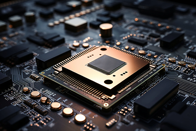
The AD9259ABCPZ-50 is housed in a 48-pin LFCSP package compliant with RoHS standards. Its operating temperature range is the industrial-grade temperature range of −40°C to +85°C.
【Core Features of the AD9259ABCPZ-50】
Four-channel synchronous sampling: Four independent ADC channels can operate simultaneously, ensuring time consistency in multi-channel signal acquisition, particularly suitable for applications requiring phase matching.
14-bit high resolution: Provides up to 73 dB signal-to-noise ratio (SNR) and 84 dBc spur-free dynamic range (SFDR), ensuring high-fidelity signal acquisition.
50MSPS high-speed sampling rate: Meets broadband signal processing requirements and is suitable for intermediate frequency sampling in communication systems.
Low-voltage serial LVDS interface: Utilises a 1.8V-powered LVDS (low-voltage differential signalling) serial interface, reducing power consumption while enhancing interference resistance.
Low power consumption design: Each channel consumes only 98mW at 50MSPS, and the power consumption is less than 2mW when the entire chip is disabled, making it suitable for portable devices.
Flexible power management: Supports independent shutdown of individual channels, allowing dynamic adjustment of power consumption according to application requirements.
【Technical specifications and performance indicators of AD9259ABCPZ-50】
Basic parameter configuration:
Resolution: 14-bit, providing 16,384 quantisation levels to ensure high-precision signal acquisition.
Sampling rate: 50 MSPS (millions of samples per second), with a maximum sampling bandwidth of 25 MHz per channel.
Number of input channels: 4 fully differential input channels, supporting synchronous sampling.
Input voltage range: 2 V p-p differential input, supporting AC or DC coupling.
Data Interface: Serial LVDS (Low Voltage Differential Signalling), compliant with the ANSI-644 standard, supporting data transfer rates up to 400 Mbps.
Power Characteristics:
Analogue Power Supply Voltage: 1.7 V to 1.9 V (typical value 1.8 V).
Digital power supply voltage: 1.7V to 1.9V (same as analogue power supply).
Power consumption: 98mW per channel (at 50MSPS), typical power consumption of 392mW when all four channels are fully operational.
Standby power consumption: Less than 2mW when all channels are disabled.
Dynamic Performance Metrics:
Signal-to-Noise Ratio (SNR): 73dB (typical value) at an input frequency of 10MHz.
Spurious-Free Dynamic Range (SFDR): 84dBc (typical value).
Effective Number of Bits (ENOB): 12 bits (at 50MSPS and 10MHz input).
Integral Nonlinearity (INL): ±3.5LSB (maximum value).
Differential Nonlinearity (DNL): ±1 LSB (maximum).
Clock and Synchronisation Characteristics:
Input Clock: Supports differential or single-ended clock input, sensitivity 50 mVpp (differential).
Clock Duty Cycle: Supports a wide range of input clock duty cycles from 30% to 70%.
Data Clock Output (DCO): Provides a data synchronisation clock for data capture at the receiving end.
Frame Clock Output (FCO): Indicates the frame start position, simplifying data alignment.
Package and Environmental Parameters:
Package Type: 48-pin LFCSP (Lead Frame Chip Scale Package), dimensions 7mm × 7mm × 0.75mm.
Pin Configuration: Includes pins for analogue input, clock, power supply, ground, LVDS data output, etc.
Operating Temperature Range: -40°C to +85°C, suitable for industrial environment applications.
ESD Protection: All pins feature 2000V HBM (human body model) ESD protection.
The AD9259ABCPZ-50 also supports multiple digital test modes, including built-in pseudo-random sequences and custom test modes, facilitating system debugging and verification. The AD9259ABCPZ-50 device offers programmable output resolution options, allowing users to balance resolution and data rate.
【Application Areas of AD9259ABCPZ-50】
AD9259ABCPZ-50 has found widespread application in multiple high-tech fields thanks to its multi-channel synchronous sampling capability and outstanding dynamic performance. As a highly integrated analogue-to-digital conversion solution, AD9259ABCPZ-50 provides a reliable data acquisition front end for various complex signal processing systems.
Medical Imaging Systems:
Ultrasound Diagnostic Equipment: The AD9259ABCPZ-50's four-channel architecture is particularly suited for multi-element receiver signal processing in medical ultrasound systems. Its high dynamic range and low noise characteristics enable clear capture of weak echo signals from human tissue, enhancing imaging quality.
Digital Beamforming: In phased array ultrasound systems, multiple AD9259ABCPZ-50 devices can work in tandem to achieve precise beam control and real-time imaging.
CT/MRI Auxiliary Circuits: Used as auxiliary data acquisition modules in medical imaging equipment, ensuring precision in the signal digitisation process.
Communication infrastructure:
Wireless base station receiver: In the intermediate frequency sampling receiver chain of 4G/5G base stations, the AD9259ABCPZ-50 can efficiently process multi-carrier signals and support MIMO (multiple input multiple output) technology.
Software-defined radio: When combined with an FPGA or DSP processor, it can build a flexible and reconfigurable radio platform to meet the needs of various communication standards.
Microwave Backhaul Equipment: Used for high-speed data acquisition and processing in point-to-point microwave communication systems.
Industrial and Test Measurement:
Non-Destructive Testing Systems: Provides high-precision echo signal digitisation in industrial ultrasonic testing, material thickness measurement, and other applications.
High-speed data acquisition cards: Used as multi-channel synchronous acquisition front-ends for test equipment such as oscilloscopes and spectrum analysers.
Vibration analysis and predictive maintenance: Synchronously acquires vibration signals from multiple sensors to monitor the health status of mechanical equipment.
Defence and Aerospace:
Radar Signal Processing: Used for synchronous acquisition and digitisation of multi-channel echo signals in phased array radar systems.
Electronic Warfare Systems: Supports real-time acquisition and analysis of broadband signals for electronic reconnaissance and countermeasures.
Satellite Communication Terminals: Provides a highly reliable ground station signal reception channel.

Time:2025-08-14
Time:2025-08-14
Time:2025-08-14
Time:2025-08-14
Contact Number:86-755-83294757
Enterprise QQ:1668527835/ 2850151598/ 2850151584/ 2850151585
Business Hours:9:00-18:00
E-mail:sales@hkmjd.com
Company Address:Room1239, Guoli building, Zhenzhong Road, Futian District, Shenzhen, Guangdong
CopyRight ©2022 Copyright belongs to Mingjiada Yue ICP Bei No. 05062024-12

Official QR Code
Links:


