Welcome Here Shenzhen Mingjiada Electronics Co., Ltd.


sales@hkmjd.com
sales@hkmjd.com


Service Telephone:86-755-83294757
 Latest Information
 Home
/Company Dynamics
/
Home
/Company Dynamics
/
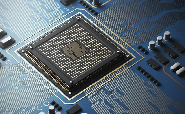
Introduction to Renesas 8T73S208B-01NLGI Buffer _ 2.5V, 3.3V Differential LVPECL Clock Buffer
8T73S208B-01NLGI is a clock buffer chip introduced by Renesas. It uses 32-VFQFN package and is mainly used to buffer and distribute clock signals. The following are its core parameters: Type: Fan-out buffer (allocation), dividerNumber of circuits: 1…
8T73S208B-01NLGI is a clock buffer chip introduced by Renesas. It uses 32-VFQFN package and is mainly used to buffer and distribute clock signals. The following are its core parameters:
Type: Fan-out buffer (allocation), divider
Number of circuits: 1
Ratio - Input: Output: 1:8
Differential - Input: Output: Yes/Yes
Input: CML, LVDS, LVPECL
Output: LVPECL
Frequency - Maximum: 1 GHz
Voltage - Power supply: 2.375V to 3.465V
Operating temperature: -40°C to 85°C
Installation type: Surface mount type
Package/Housing: 32-VFQFN

Introduction
The 8T73S208B-01NLGI is a high-performance differential LVPECL clock divider and fan-out buffer. This device is designed for frequency division and signal fan-out of high-frequency, low-phase noise clocks. The 8T73S208B-01NLGI is characterized by its operation under 2.5V and 3.3V power supplies. The guaranteed output-to-output and part-to-part skew characteristics make the 8T73S208B-01NLGI an ideal choice for clock distribution applications that require clear performance and repeatability.
In addition, the integrated input terminal resistor of the 8T73S208B-01NLGI makes the interface with the reference source easy and reduces the number of passive components. Each output can be enabled or disabled independently in a high-impedance state controlled by the I2C register. When powered on, all outputs are disabled.
Main features
A differential input reference clock
The differential pair can accept the following differential input levels :LVDS, LVPECL, CML
Integrated input terminal resistor
8-channel LVPECL output
The optional clock divisions are 1, 2, 4 and 8
Maximum input clock frequency :1GHz
Control the level of the LVCMOS interface input
Enable/Disable independent output through the I2C interface
Power-on status: All outputs are disabled
Output skew :60ps(maximum)
Output rise/fall time :350ps(maximum value)
Low additive phase jitter, root mean square :182fs(typical value)
Full 2.5V and 3.3V power supply voltages
Lead-free (RoHS 6) 32-pin VFQFN package
The operating temperature range is from -40°C to 85°C
Application scenarios
8T73S208B-01NLGI achieves buffering and distribution of clock signals through differential signals, mainly including:
High-speed communication systems : such as clock signal distribution and synchronization for 5G communication base stations and data centers.
Industrial control : clock buffer management for PLCS and automated equipment.
Video processing system: Clock signal distribution and anti-interference processing for high-definition display devices and video transmission equipment.
Get your exclusive quotation plan for 8T73S208B-01NLGI right away
Sales Hotline: +86 13410018555 (Mr. Chen)
Service email: sales@hkmjd.com
For more information, please visit www.hkmjd.com
![[TI] INA193AIDBVR 500kHz Current Sense Amplifiers——Current Shunt Monitor](/upload/202508/25/202508251455390711.jpg)
Time:2025-08-25
![[Genuine Original Product] Infineon IGBT Module_FZ900R12KE4_1200V/900A Industrial Grade](/upload/202508/25/202508251435528213.jpg)
Time:2025-08-25
Time:2025-08-25
Time:2025-08-25
Contact Number:86-755-83294757
Enterprise QQ:1668527835/ 2850151598/ 2850151584/ 2850151585
Business Hours:9:00-18:00
E-mail:sales@hkmjd.com
Company Address:Room1239, Guoli building, Zhenzhong Road, Futian District, Shenzhen, Guangdong
CopyRight ©2022 Copyright belongs to Mingjiada Yue ICP Bei No. 05062024-12

Official QR Code
Links:


