Welcome Here Shenzhen Mingjiada Electronics Co., Ltd.

sales@hkmjd.com

sales@hkmjd.com

Service Telephone:86-755-83294757
 Latest Information
 Home
/Industry Information
/
NOVOSENSE Launches Automotive-Grade Isolated Half-Bridge Driver Series with Miller Clamp Function
NOVOSENSE Electronics has officially launched the NSI6602MxEx series of automotive-grade isolated half-bridge driver chips. Building on the classic NSI6602 product, this series innovatively integrates a 5A Miller clamp function and features high isola…
NOVOSENSE Electronics has officially launched the NSI6602MxEx series of automotive-grade isolated half-bridge driver chips. Building on the classic NSI6602 product, this series innovatively integrates a 5A Miller clamp function and features high isolation voltage withstand capability, low latency, and programmable dead time. It is specifically designed for power devices such as SiC (silicon carbide) and IGBT, and is suitable for high-reliability applications such as OBC (on-board chargers), DC/DC converters, active suspension systems, and other high-reliability applications.

Comparison of NSI6602MxEx and NSI6602 functional block diagrams
5A Miller clamping function enhances the safety and reliability of half-bridge circuits
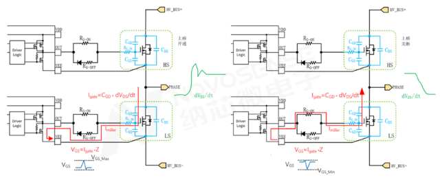
In practical applications, power devices in bridge circuits such as OBC/DC-DC converters, industrial power supplies, and motor drives are prone to crosstalk behaviour. Especially with the adoption of third-generation power devices like SiC and GaN, both the gate threshold voltage and maximum withstand reverse voltage have decreased, reducing the voltage margin available to suppress parasitic conduction. When using traditional half-bridge driver chips, adjustments to the driver circuit are typically required to avoid bridge arm shorting caused by the Miller effect.
However, in many cases, even after carefully adjusting driver parameters, positive and negative supply voltages, and optimising PCB gate parasitic parameters, it is difficult to simultaneously control positive and negative crosstalk within safe margins. This not only limits the performance of devices like silicon carbide but may also pose potential safety hazards.

Principle of the Miller effect during switching
NOVOSENSE has launched the NSI6602MxEx series, which integrates a 5A-capable Miller clamping function into a two-channel half-bridge drive circuit. This provides a path of minimum impedance for Miller current release, effectively suppressing the rise in crosstalk voltage. The NSI6602MxEx is fully equipped based on the NSI6602, ensuring safe application of devices like SiC.
Application Sharing of the NSI6602MxEx Miller Clamping Solution
When using SiC power devices, due to their high dv/dt characteristics, the gate often experiences positive and negative crosstalk voltages (Vswing) whose amplitudes exceed the gate threshold voltage (Vgsth) and the negative voltage withstand limit (Vgs_min). This crosstalk can easily cause misfiring or device damage, posing a significant challenge for high-performance driver design.
±10A Output Current Enables Simplified Peripheral Circuit Design
The NSI6602MxEx offers exceptional drive capability, supporting a maximum output current of 10A and rail-to-rail output. Whether directly driving power transistors with larger gate charge (Qg) or in multi-transistor parallel applications, the NSI6602MxEx eliminates the need for additional buffers compared to traditional solutions, enabling efficient drive performance and significantly simplifying peripheral circuit design. Additionally, with a maximum operating voltage of 32V and a maximum withstand voltage of 35V, it can withstand higher EOS impacts. Combined with a simplified drive peripheral design, this significantly enhances the reliability of the entire circuit system.
Programmable dead time and multi-level undervoltage thresholds enable flexible design configuration
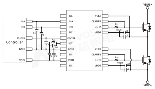
The NSI6602MxEx supports dead-time configuration via the DT pin, allowing flexible adjustment of dead-time durations by modifying the pull-down resistor. Additionally, the DT pin can be directly connected to the primary-side VCC for parallel output from two drivers. Combined with two selectable enable logic options (DIS/EN), it provides rich control logic for end-application requirements. Furthermore, the secondary-side power supply undervoltage UVLO offers three options: 8V, 12V, and 17V, accommodating undervoltage protection in various power design scenarios for IGBT and SiC applications.
NSI6602MxEx product features:
5700VRMS isolation voltage rating, capable of driving high-voltage SiC and IGBT
High CMTI: 150 kV/μs
Input side power supply voltage: 3V to 18V
Drive side power supply voltage: up to 32V
Rail-to-rail output
Peak sink/source current: ±10A
Peak Miller clamp current: 5A
Drive power supply under-voltage: 8V/12V/17V three-level selectable
Programmable dead-time
Selectable positive/negative logic enable configuration
Typical propagation delay: 80ns
Operating temperature range: -40°C to 125°C
Compliant with the AEC-Q100 standard for automotive applications
RoHS-compliant package type: SOW18, creepage distance >8mm

Typical application circuit
Product selection and packaging
The NSI6602MxEx series offers six models to choose from, featuring a wide range of enable logic configurations and drive power supply under-voltage specifications, providing flexible adaptation to various application scenarios.

![[RF] SYM-2500 mixer-supports RF signal processing from 1 MHz to 2.5 GHz](/upload/202508/18/202508181218146815.png)
Time:2025-08-18

Time:2025-08-18

Time:2025-08-18

Time:2025-08-18
Contact Number:86-755-83294757
Enterprise QQ:1668527835/ 2850151598/ 2850151584/ 2850151585
Business Hours:9:00-18:00
E-mail:sales@hkmjd.com
Company Address:Room1239, Guoli building, Zhenzhong Road, Futian District, Shenzhen, Guangdong
CopyRight ©2022 Copyright belongs to Mingjiada Yue ICP Bei No. 05062024-12

Official QR Code
Links: