Welcome Here Shenzhen Mingjiada Electronics Co., Ltd.

sales@hkmjd.com

sales@hkmjd.com

Service Telephone:86-755-83294757
 Latest Information
 Home
/Company Dynamics
/
AD9250BCPZ-250 Analog-to-Digital Converter Features 250 MSPS, JESD204B, 14-Bit Dual ADC
The AD9250BCPZ-250 is a dual-channel 14-bit analog-to-digital converter (ADC) launched by Analog Devices (ADI), featuring a sampling rate of 250 MSPS. It adopts the JESD204B high-speed serial interface and supports dual-channel synchronous sampling. Y…
The AD9250BCPZ-250 is a dual-channel 14-bit analog-to-digital converter (ADC) launched by Analog Devices (ADI), featuring a sampling rate of 250 MSPS. It adopts the JESD204B high-speed serial interface and supports dual-channel synchronous sampling. Youdaoplaceholder0 the following are its core advantages:
Integrated dual-channel, 14-bit, 250 MSPS ADC.
The configurable JESD204B output module supports a maximum sampling rate of 5 Gbps per channel.
The on-chip phase-locked loop (PLL) enables users to provide a single ADC sampling clock, and the corresponding JESD204B data rate clock is generated by multiplying the PLL by this ADC sampling clock.
Support optional RF clock input to simplify the system board design.
The patented differential input maintains excellent signal-to-noise ratio (SNR) performance even at input frequencies up to 400 MHz.
It is powered by a single 1.8V power supply.
The Standard Serial Port Interface (SPI) supports various product features and functions, such as: control clock DCS, power-saving mode, test mode, reference voltage mode, rapid out-of-range detection, and serial output configuration, etc.

Explanation
The AD9250BCPZ-250 is a dual-channel 14-bit ADC with a maximum sampling rate of 250 MSPS, designed to provide solutions for low-cost, small-sized, wide-bandwidth, and multi-functional communication applications.
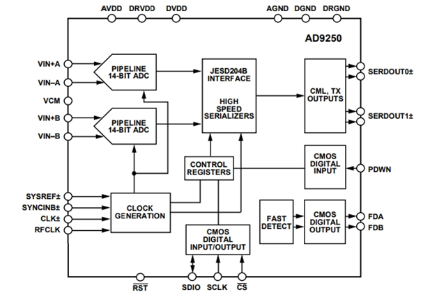
The core of AD9250BCPZ-250 adopts a multi-level, differential pipeline architecture and integrates output error correction logic. The ADC core features a wide bandwidth input and supports various input ranges selectable by users. Integrated reference voltage sources can simplify the design. Duty cycle stabilizers can be used to compensate for the fluctuations in the duty cycle of the ADC clock, enabling the converter to maintain excellent performance. The JESD204B high-speed serial interface can reduce the wiring requirements of circuit boards and decrease the number of pins needed for receiving devices.
By default, the output data of AD9250BCPZ-250 is directly routed to two JESD204B serial output channels, which are set to CML level. The four modes support any combination of M = 1 or 2 (single-channel or dual-channel converter) and L = 1 or 2 (single-channel or dual-channel). In dual-channel ADC mode, data can be sent through two channels at a maximum sampling rate of 250 MSPS. However, if data is sent through a single channel, only a maximum sampling rate of 125 MSPS is supported. The device provides synchronous inputs (SYNCINB± and SYSREF±).
When necessary, the flexible shutdown option of the AD9250BCPZ-250 can significantly reduce power consumption. Each channel supports programmable out-of-range level detection through a dedicated fast detection pin. Settings and control programming are accomplished using a three-wire SPI-compatible serial interface.
The AD9250BCPZ-250 is packaged in a 48-pin LFCSP package and has a rated temperature range of -40 °C to +85°C in the industrial temperature range.
Application field
The AD9250BCPZ-250 is suitable for fields such as wireless communication (such as 3G/4G/5G base stations, WiMax), radar systems, industrial automation, and test and measurement, and supports high-speed signal processing requirements. Youdaoplaceholder0 mainly includes
Diversity radio system
Multimode digital receiver (3G), TD-SCDMA, WiMax, WCDMA, CDMA2000, GSM, EDGE, LTE
HFC digital reverse path receiver
I/Q demodulation system
Intelligent antenna system
Electronic test and measurement equipment
Radar receiver
COMSEC radio architecture
IED detection/interference system
General Software-defined Radio
Broadband Data application
The main features of AD9250BCPZ-250 include:
JESD204B Subclass 0 or Subclass 1 encodes serial digital output
The signal-to-noise ratio (SNR) at 185 MHz AIN is 70.6 dBFS
No. 250
The spurious dynamic range (SFDR) at 185 MHz is 88 dBc
Ain and 250 MSPS Street
Total power consumption: 711 megawatts at 250 MSPS
1.8V power supply voltage
Input integers 1 to 8 into the clock divider
A sampling rate of up to 250 MSPS
A maximum intermediate frequency sampling rate of 400 MHz
Internal analog-to-digital converter (ADC) reference voltage source
Flexible analog input range
Peak value from 1.4V to 2.0V (nominal value is 1.75V peak value)
ADC Clock Duty cycle Stabilizer (DCS
95 dB channel isolation/crosstalk
Serial port control
Energy-saving and power-saving mode

Immediately visit the official website of Mingjiada (www.hkmjd.com) to obtain the exclusive product quotation of AD9250BCPZ-250.
![Recycle Microcontroller MCU, Recycle [GigaDevice] GD32E502 Series Microcontrollers](/upload/202509/01/202509011540143370.jpg)
Time:2025-09-01

Time:2025-09-01

Time:2025-09-01

Time:2025-09-01
Contact Number:86-755-83294757
Enterprise QQ:1668527835/ 2850151598/ 2850151584/ 2850151585
Business Hours:9:00-18:00
E-mail:sales@hkmjd.com
Company Address:Room1239, Guoli building, Zhenzhong Road, Futian District, Shenzhen, Guangdong
CopyRight ©2022 Copyright belongs to Mingjiada Yue ICP Bei No. 05062024-12

Official QR Code
Links: