Welcome Here Shenzhen Mingjiada Electronics Co., Ltd.

sales@hkmjd.com

sales@hkmjd.com

Service Telephone:86-755-83294757
 Latest Information
 Home
/Company Dynamics
/
A fan-out buffer and crossover that complies with the JESD204B standard: 8V79S680NLGI [Renesas]
The 8V79S680NLGI is a fandout buffer and frequency divider that complies with the JESD204B standard, mainly applied in scenarios of clock signal distribution and frequency conversion. The following are its core parameters and features:Supports high-sp…
The 8V79S680NLGI is a fandout buffer and frequency divider that complies with the JESD204B standard, mainly applied in scenarios of clock signal distribution and frequency conversion. The following are its core parameters and features:
Supports high-speed, low-phase noise converter clock
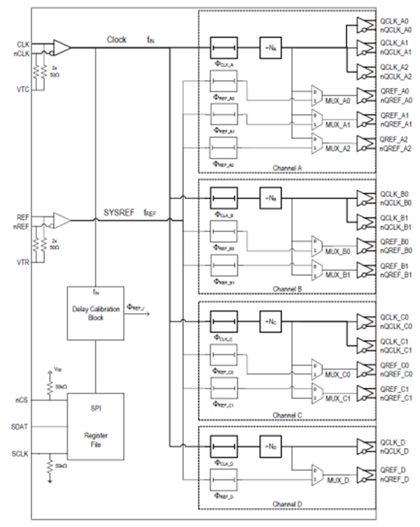
The distribution, fan-out and phase delay of clock and SYSREF signals
Extremely low output background noise: -158.8dBc/Hz background noise (245.76MHz)
Supports clock frequencies up to 3GHz, including clock output frequencies of 983.04MHz, 491.52MHz, 245.76MHz and 122.88MHz
4 output channels, with a total of 16 differential outputs:
-8 dedicated clock outputs
The 8 outputs can be configured as SYSREF outputs with independent phase delay stages or as additional clock outputs
Each channel contains:
- Frequency divider: ÷1, ÷2, ÷4, ÷6, ÷8, ÷12, ÷16
-Clock phase delay circuit
Clock phase delay circuit
- Clock: The delay unit is the clock cycle; 256 steps
-SYSREF: Configurable precision phase delay circuit: 8-stage 131ps, 262ps, 393ps or 524ps
Flexible differential output
-LVDS /LVPECL is configurable
- Amplitude is configurable
- Power-saving mode without using the output
- Supports DC and AC coupling
The QREF (SYSREF) output pre-bias function can prevent malfunctions when the output is turned on or off
Power supply voltage
-3.3V core and signal I/O
-1.8V digital control SPI I/O (3.3V tolerance input)
64 VFQFN-P package (9mm x 9mm x 0.85mm)
Ambient temperature range: -40°C to +85°C

For details
The 8V79S680NLGI is a high-performance clock and converter synchronization solution specifically designed for circuit boards of wireless base station radio equipment, conforming to JESD204B Subclass 0, 1 and 2 standards. The main function of the 8V79S680NLGI is to distribute and fan out the high-frequency clock and low-frequency system reference signals generated by the JESB204B clock generator (such as the 8V19N480), thereby expanding its fan out function and providing additional phase delay. The 8V79S680NLGI has been optimized to provide A clock with extremely low phase noise and precise, phase-adjustable SYSREF synchronization signals, meeting the implementation requirements of GSM, WCDMA, LTE, and LTE-A radio boards. Low offset output, low inter-device offset characteristics, and fast output rise/fall times help the system design achieve deterministic clock and SYSREF phase relationships across devices.
The 8V79S680NLGI distributes the input clock and JESD204B SYSREF signal to four fan-out channels. In each channel, the input clock and SYSREF signals are fan-out to multiple clock (QCLK) and SYSREF (QREF) outputs. Clock signals can be frequency-divided in each channel. Configurable phase delay circuits can be used for clock and SYSREF signals. The propagation delay in all signal paths is completely determined to support the fixed phase relationship between the clock and the SYSREF signal within a device. The clock divider can be bypassed to achieve a low-latency clock path. The 8V79S680NLGI can assist in achieving synchronization among some frequency dividers within the device and among multiple devices, eliminating the phase ambiguity introduced by the frequency divider between the power supply and configuration cycles.
Each channel supports a clock frequency of up to 3GHz. In another configuration, such as JESD204B subclasses 0 and 2, the SYSREF (QREF) output can be configured as a regular clock output, thereby adding additional clock fan-out to the device.
All outputs are highly flexible in terms of amplitude configuration and output signal termination, and allow for both DC and AC coupling. When not in use, you can disable the output and turn off the power. The SYSREF output pre-bias function can prevent startup failures and achieve AC coupling of system synchronization signals.
The 8V79S680NLGI is configured via a three-wire SPI serial interface. This device adopts a lead-free (RoHS 6) 64-pin VFQFN package. The extended temperature range supports the requirements of wireless infrastructure, telecommunications and network terminal devices. The 8V79S680NLGI belongs to the IDT high-performance clock series.
Typical applications
▪ JESD204B low phase noise clock and SYSREF signal distribution
▪ Support for JESD204 subclasses 0, 1, and 2
▪ Clock distribution devices for jitter sensitive ADC and DAC circuits
▪ Wireless infrastructure
▪ Radar and imaging
▪ Instrumentation and medical care
Contact Mingjiada (www.hkmjd.com) immediately for an exclusive quote on the 8V79S680NLGI clock buffer!
![[In Stock] Supply AM26LV32EIPWR (TI) Quadruple Differential Line Receiver](/upload/202508/26/202508261500001884.jpg)
Time:2025-08-26

Time:2025-08-26

Time:2025-08-26
![Supply [Onsemi] MOSFETs, Mingjiada Supply Power MOSFET, Silicon Carbide (SiC) MOSFET](/upload/202508/26/202508261411186598.jpg)
Time:2025-08-26
Contact Number:86-755-83294757
Enterprise QQ:1668527835/ 2850151598/ 2850151584/ 2850151585
Business Hours:9:00-18:00
E-mail:sales@hkmjd.com
Company Address:Room1239, Guoli building, Zhenzhong Road, Futian District, Shenzhen, Guangdong
CopyRight ©2022 Copyright belongs to Mingjiada Yue ICP Bei No. 05062024-12

Official QR Code
Links: