Welcome Here Shenzhen Mingjiada Electronics Co., Ltd.

sales@hkmjd.com

sales@hkmjd.com

Service Telephone:86-755-83294757
 Latest Information
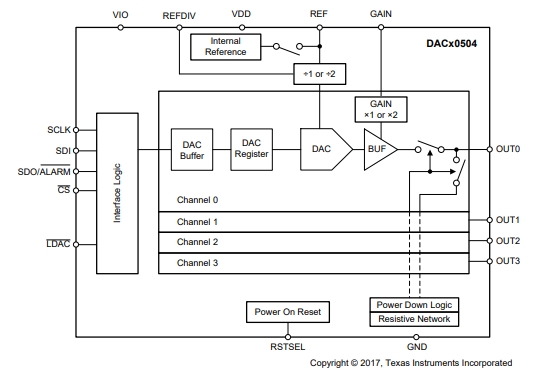
The DAC80504RTER device is a four-channel 16-bit SPI voltage output digital-to-analog converter (DAC) with an internal reference voltage. This device mainly has the following features:Performance-INL: 1 LSB (maximum value) at 16-bit resolution-TUE: FS…
The DAC80504RTER device is a four-channel 16-bit SPI voltage output digital-to-analog converter (DAC) with an internal reference voltage. This device mainly has the following features:
Performance
-INL: ±1 LSB (maximum value) at 16-bit resolution
-TUE: FSR maximum value ±0.1%
Integrate a 2.5V precise internal reference voltage
- Initial accuracy: ±5 mV, maximum value
-Low temperature drift: 2ppm/°C (typical value)
• High driving capacity: 20mA 0.5V power rail
Flexible output configuration
- User-selectable gains: 2, 1 or ½
- Reset to zero scale or calibration
• Wide operating range:
- Power supply: 2.7V to 5.5V
-Temperature: -40 ° C to +125 ° C
50MHz, SPI-compatible serial interface
- 4-wire mode, operating voltage 1.7V to 5.5V
-The chrysanthemum chain is running
-CRC error check
• Low power consumption: 0.7mA/ channel (5.5V)
• Small package: 3mm × 3mm, 16-pin WQFN

Details
The DAC80504RTER is a low-power, four-channel, buffered voltage output digital-to-analog converter (DAC) with 16-bit resolution. The DAC80504RTER features a low-drift 2.5V internal reference voltage, eliminating the need for an external accuracy reference in most applications. The user-selectable gain configuration provides full-scale output voltages of 1.25V (gain = ½), 2.5V (gain = 1), or 5V (gain = 2). These devices are powered by a single power supply ranging from 2.7V to 5.5V, have specified monotonicity, and can provide a high linearity of ±1LSB INL.
Communicate with the DAC80504RTER through a 4-wire serial interface with an operating clock rate of 50MHz. The VIO pin enables the serial interface to operate within a voltage range of 1.7V to 5.5V. The flexible interface of DAC80504RTER enables it to be used in a wide range of industry-standard microprocessors and microcontrollers.
The DAC80504RTER adopts a power-on reset circuit. After power-on, it can keep the DAC output at zero level or intermediate level until a valid code is written into the device. This device consumes a low current of 0.7mA per channel at 5.5V, and thus is highly suitable for battery-powered devices. The power-off characteristic of each channel can reduce the current consumption of the device to 15µA.
The DAC80504RTER can operate normally within a temperature range of -40 °C to +125°C and is available in a 3mm × 3mm QFN compact package.
Application scenarios
The DAC80504RTER is suitable for application scenarios that require high-precision and multi-channel analog-to-digital conversion, such as:
Optical fiber network
Wireless infrastructure
"Industrial automation"
• Data acquisition system
Technical Specification
Product: DAC80504RTER
Number of digits: 16
Digital-to-analog converter number: 4
Establishment time: 5µs (typical value)
Output type: Voltage-Buffered
Differential output: None
Data interface: SPI
Reference type: Internal
Voltage - Power supply, simulation: 2.7V to 5.5V
Voltage - Power supply, digital: 2.7V to 5.5V
INL/DNL (LSB) : ±0.5, ±0.5
Architecture: R-2R
Operating temperature: -40°C to 125°C
Package/Shell: 16-WFQFN
Act now and visit Mingjia Da (www.hkmjd.com) for an exclusive quote on the DAC80504RTER!
![[Supply Ethernet IC] Supply Infineon——Ethernet Bridge/Ethernet PHY/Ethernet Switch](/upload/202509/09/202509091206530131.jpg)
Time:2025-09-09

Time:2025-09-09

Time:2025-09-09

Time:2025-09-09
Contact Number:86-755-83294757
Enterprise QQ:1668527835/ 2850151598/ 2850151584/ 2850151585
Business Hours:9:00-18:00
E-mail:sales@hkmjd.com
Company Address:Room1239, Guoli building, Zhenzhong Road, Futian District, Shenzhen, Guangdong
CopyRight ©2022 Copyright belongs to Mingjiada Yue ICP Bei No. 05062024-12

Official QR Code
Links: