Welcome Here Shenzhen Mingjiada Electronics Co., Ltd.


sales@hkmjd.com
sales@hkmjd.com


Service Telephone:86-755-83294757
 Latest Information
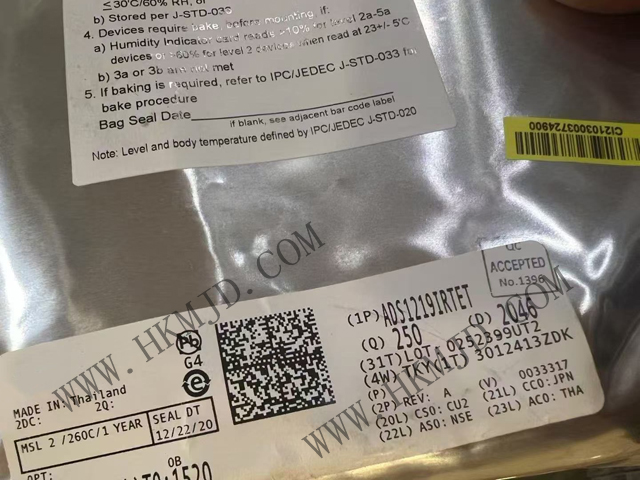
Product introductionThe LMK1D2108 clock buffer allocates two clock inputs (IN0 and IN1) to 16 pairs of differential LVDS clock outputs (OUT0 to OUT15), achieving clock allocation with ultra-small delays. Each buffer block consists of one input and up …
Product introduction
The LMK1D2108 clock buffer allocates two clock inputs (IN0 and IN1) to 16 pairs of differential LVDS clock outputs (OUT0 to OUT15), achieving clock allocation with ultra-small delays. Each buffer block consists of one input and up to eight LVDS outputs. Inputs can be LVDS, LVPECL, HCSL, CML, or LVCMOS.
The LMK1D2108 is designed to drive 50Ω transmission lines. When driving the input in single-ended mode, apply an appropriate bias voltage to the unused negative input pin.
Output groups can be enabled or disabled using the control pin (EN). If the pin remains open, two sets of outputs are enabled. If the control pin switches to logic "0", both sets of outputs are disabled (static logic "0"). If the control pin switches to logical "1", the output of one group is disabled and the output of the other group is enabled. The device also supports fail-safe functionality. The device also incorporates input hysteresis to prevent random output oscillations in the absence of an input signal.
Features
• High performance LVDS clock buffer series: up to 2GHz
- Dual 1:6 differential buffer
- Dual 1:8 differential buffer
• Supply voltage: 1.71V to 3.465V
• Low additional jitter: less than the maximum 60fs RMS in the range of 12kHz to 20MHz at 156.25MHz
- Ultra-low phase background noise: -164 DBC /Hz (typical)
• Ultra-low propagation delay: < 575ps (Max)
• Output delay: 20ps (Max)
• High swing LVDS (boost mode) : 500mV VOD (typical value, when AMP_SEL is set to 1)
• Enable/disable groups using EN pins
• Failsafe input operation
• Universal input accepts LVDS, LVPECL, LVCMOS, HCSL and CML signal levels
• LVDS reference voltage (VAC_REF) is suitable for capacitatively coupled inputs
• Industrial temperature range: -40 °C to 105°C
• Package: 7mm x 7mm 48-pin VQFN(RGZ)
Applications
• Telecommunications and networking
• Medical Imaging
• Test and measurement
• Wireless infrastructure
• Professional audio, video and signage
Mingjiada Electronics (recycling) supplies TI LMK1D2108RGZR LVDS buffer with low additional jitter. If you need it, please contact us.
Contact: Mr. Chen
Tel: +8613410018555
Email: sales@hkmjd.com

Time:2025-08-15

Time:2025-08-15
Time:2025-08-15
![[Supply Original] RAA2116514GNP (Renesas) Integrated 60V, 5A Synchronous Buck Regulator](/upload/202508/15/202508151442135784.jpg)
Time:2025-08-15
Contact Number:86-755-83294757
Enterprise QQ:1668527835/ 2850151598/ 2850151584/ 2850151585
Business Hours:9:00-18:00
E-mail:sales@hkmjd.com
Company Address:Room1239, Guoli building, Zhenzhong Road, Futian District, Shenzhen, Guangdong
CopyRight ©2022 Copyright belongs to Mingjiada Yue ICP Bei No. 05062024-12

Official QR Code
Links:


