Welcome Here Shenzhen Mingjiada Electronics Co., Ltd.

sales@hkmjd.com

sales@hkmjd.com

Service Telephone:86-755-83294757
 Latest Information
 Home
/Company Dynamics
/
ADI LTC2311CMSE-14 (Analog-to-Digital Converter): 14-Bit Sign Bit, 5Msps Differential Input ADC
Ltc2311cmse-14:14-bit signed bit, 5Msps differential input ADC1. Basic parametersModel: LTC2311CMSE-14Digit number: 14Sampling rate (per second) : 5MInput number: 1Input type: DifferentialData interface: LVDS - Serial, SPIConfiguration: S/H-ADCRatio -…
Ltc2311cmse-14:14-bit signed bit, 5Msps differential input ADC
1. Basic parameters
Model: LTC2311CMSE-14
Digit number: 14
Sampling rate (per second) : 5M
Input number: 1
Input type: Differential
Data interface: LVDS - Serial, SPI
Configuration: S/H-ADC
Ratio -S /H:ADC: 1:1
Number of A/D converters: 1
Architecture: SAR
Reference types: External, Internal
Voltage - Power supply, simulation: 3.13V - 3.47V, 5V
Voltage - Power supply, figures: 3.13V to 3.47V, 5V
Feature: -
Operating temperature: 0°C to 70°C
Package/Shell: 16-MSOP
Installation type: Surface mount type

2. Explanation
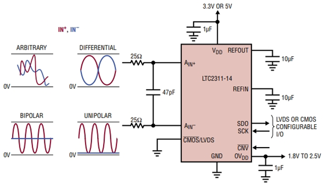
The LTC2311CMSE-14 is a low-noise, high-speed, 14-bit signed bit successive approximation register (SAR) ADC with differential input and wide input common-mode range. The LTC2311CMSE-14 adopts a single 3.3V or 5V working power supply and has an 8VP-P differential input range, making it highly suitable for applications that require a wide dynamic range and high common-mode rejection. The LTC2311CMSE-14 achieved ±0.75LSB INL (typical value), no missed code (at 14 bits), and 80dB SNR (typical value).
The LTC2311CMSE-14 has a built-in low-drift (maximum value of 20ppm/°C) 2.048V or 4.096V temperature-compensated reference, and provides an external 1.25V buffered reference input. In addition, the LTC2311CMSE-14 also has a high-speed SPI-compatible serial interface that supports CMOS or LVDS. The high throughput rate of 5Msps and the single-cycle delay characteristics make the LTC2311CMSE-14 an ideal choice for numerous high-speed applications. The LTC2311CMSE-14 consumes only 50mW of power when using a 5V power supply and provides dozing and sleeping modes to reduce power consumption to 5μW, thereby achieving the purpose of further power saving during standby.
3. The main features of LTC2311CMSE-14 include:
Throughput rate: 5Msps
Ensure ±0.75LSB INL (typical value) and ±2LSB INL
Ensure 14 digits and no code loss
An 8VP-P differential input with a wide input common-mode range
80dB SNR (typical value, fIN = 2.2MHz)
-90 dB THD (typical value, fIN = 2.2MHz)
The guaranteed operating temperature range is from -40 °C to 125°C
3.3V or 5V single power supply
Low drift (up to 20ppm/°C) 2.048V or 4.096V internal reference voltage source, with 1.25V external reference voltage source input
I/O voltage range: 1.8V to 2.5V
Serial I/O compatible with CMOS or LVDS SPI
Power consumption: 50mW (VDD = 5V, typical value)
Small 16-pin (4mm × 5mm) MSOP package
Complies with the EC-Q100 standard and is suitable for automotive applications
3. Application fields of LTC2311CMSE-14:
High-speed data acquisition system
Communication
Remote data acquisition
Imaging
Optical network
Automobile
Multiphase motor control
Consult Mingjiada Electronics immediately to obtain the exclusive quotation for LTC2311CMSE-14!
Website: www.hkmjd.com | Email: sales@hkmjd.com

Time:2025-07-21

Time:2025-07-21
![[Supply/Recycling] IGBT Module: Mitsubishi Electric CM900HG-130X HVIGBT X Series Power Module](/upload/202507/21/202507211506358351.jpg)
Time:2025-07-21
![Supply [ADI] LDO Linear Regulators, LED Driver IC, Battery Management IC](/upload/202507/21/202507211436467273.jpg)
Time:2025-07-21
Contact Number:86-755-83294757
Enterprise QQ:1668527835/ 2850151598/ 2850151584/ 2850151585
Business Hours:9:00-18:00
E-mail:sales@hkmjd.com
Company Address:Room1239, Guoli building, Zhenzhong Road, Futian District, Shenzhen, Guangdong
CopyRight ©2022 Copyright belongs to Mingjiada Yue ICP Bei No. 05062024-12

Official QR Code
Links: