Welcome Here Shenzhen Mingjiada Electronics Co., Ltd.

sales@hkmjd.com

sales@hkmjd.com

Service Telephone:86-755-83294757
 Latest Information
 Home
/Company Dynamics
/
Supply RF Front End ADRF5545ABCPZN ADRF5545 Dual Channel 2.4 GHz to 4.2 GHz Receiver Front End
Shenzhen Mingjiada Electronics Co., Ltd. new and original supply of RF front-end ADRF5545ABCPZN ADRF5545 dual-channel 2.4 GHz to 4.2 GHz receiver front-endADRF5545ABCPZN Overview:Product DetailsThe ADRF5545A is a dual-channel integrated radio frequenc…
Shenzhen Mingjiada Electronics Co., Ltd. new and original supply of RF front-end ADRF5545ABCPZN ADRF5545 dual-channel 2.4 GHz to 4.2 GHz receiver front-end
ADRF5545ABCPZN Overview:
Product Details
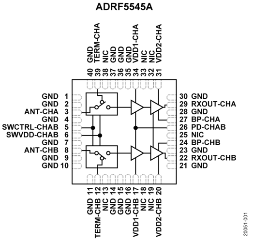
The ADRF5545A is a dual-channel integrated radio frequency (RF) front-end multi-chip module designed for time division duplex (TDD) applications operating from 2.4 GHz to 4.2 GHz. The ADRF5545A is a dual-channel configuration containing a cascaded two-stage low noise amplifier (LNA) and a high-power silicon single knife double throw (SPDT) switch.
In high gain mode, the cascaded two-stage LNA and switch provide a low noise figure (NF) of 1.45 dB and a high gain of 32 dB at 3.6 GHz and an output 3rd order intermodulation point (OIP3) of 32 dBm (typical). In low gain mode, one of the two LNA stages is bypassed, providing 16 dB of gain at a lower current of 36 mA. In off mode, the LNA is switched off and the device current consumption is 12 mA.
During transmit, the switch provides a low insertion loss of 0.65 dB when the RF input is connected to the end electrode pin (TERM-ChA or TERM-ChB) and handles 40 dBm of Long Term Evolution (LTE) average power (9 dB peak/average ratio (PAR)) over its lifetime, compared to 43 dBm in single event (<10 seconds) LNA protection mode. dBm.
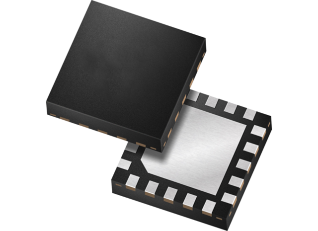
The device is available in a compact 6 mm × 6 mm 40-pin RoHS-compliant LFCSP package.
Device Applications
Wireless infrastructure
TDD large-scale multi-input and multi-output and active antenna systems
TDD-based communication systems

Features and benefits
Integrated dual-channel RF front-end
2-stage LNA and high power SPDT switch
On-chip biasing and matching
Single power supply
Gain
High gain mode: 32 dB (typical) at 3.6 GHz
Low gain mode: 16 dB (typ.) at 3.6 GHz
Low noise index
High gain mode: 1.45 dB (typ.) at 3.6 GHz
Low gain mode: 1.45 dB (typ.) at 3.6 GHz
High isolation
RXOUT-CHA and RXOUT-CHB: 47 dB (typ.)
TERM-CHA and TERM-CHB: 52 dB (typ.)
Low insertion loss: 0.65 dB (typ.) at 3.6 GHz
High power handling capability at TCASE = 105°C
Full lifecycle
LTE average power (9 dB PAR): 40 dBm
Single event (<10 sec run)
LTE average power (9 dB PAR): 43 dBm
High OIP3: 32 dBm (typical)
Off mode and low gain mode (for LNA)
Low supply current
High gain mode: 86 mA at 5 V (typical)
Low gain mode: 36 mA (typ.) at 5 V
Off mode: 12 mA (typ.) at 5 V
Positive logic control
6 mm × 6 mm 40-pin LFCSP package
Quality assurance, real single friends with accepted price please call for advice: QQ: 1668527835
Tel: +8613410018555
E-mail: sales@hkmjd.com
Company Home: www.hkmjd.com

Time:2025-08-23

Time:2025-08-23

Time:2025-08-23

Time:2025-08-23
Contact Number:86-755-83294757
Enterprise QQ:1668527835/ 2850151598/ 2850151584/ 2850151585
Business Hours:9:00-18:00
E-mail:sales@hkmjd.com
Company Address:Room1239, Guoli building, Zhenzhong Road, Futian District, Shenzhen, Guangdong
CopyRight ©2022 Copyright belongs to Mingjiada Yue ICP Bei No. 05062024-12

Official QR Code
Links: