Welcome Here Shenzhen Mingjiada Electronics Co., Ltd.

sales@hkmjd.com

sales@hkmjd.com

Service Telephone:86-755-83294757
 Latest Information
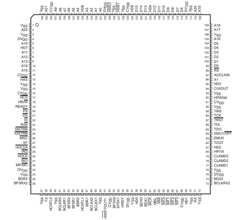
The TMS320VC5407PGE digital signal processor is based on an advanced and improved Harvard architecture with one program memory bus and three data memory buses. These processors provide highly parallelized arithmetic logic units (ALUs), application-spe…
The TMS320VC5407PGE digital signal processor is based on an advanced and improved Harvard architecture with one program memory bus and three data memory buses. These processors provide highly parallelized arithmetic logic units (ALUs), application-specific hardware logic, on-chip memory, and additional on-chip peripherals. The operational flexibility and speed of these DSPS are based on highly specialized instruction sets.
Separate program and data Spaces allow simultaneous access to program instructions and data, providing a high degree of parallelism. Two read operations and one write operation can be performed in a single cycle. Instructions with parallel storage and application-specific instructions can take full advantage of this architecture. In addition, data can be transferred between data and program space. This parallelism supports a powerful set of arithmetic, logical, and bit-manipulation operations that can all be performed in a single machine cycle. These DSPS also include control mechanisms to manage interrupts, repetitive operations, and function calls.
Product: TMS320VC5407PGE
Core: C54x
Clock frequency: 120MHz
Package: LQFP-144

Features:
Advanced multibus architecture with three separate 16-bit data memory buses and one program memory bus
The 40-bit arithmetic logic Unit (ALU) consists of a 40-bit barrel shifter and two independent 40-bit accumulators
The 17-× 17-bit parallel multiplier is coupled to a 40-bit dedicated adder for non-pipelined single-cycle multiply/accumulate (MAC) operations
Compare, Select, and store units (CSSUs) for add/compare selection of Viterbi operators
The index encoder calculates the value of the index value of 40 single-cycle bit accumulator
Two address generators with 8 secondary registers and 2 secondary register arithmetic units (ARAU)
A data bus with a bus holder function
Extended addressing mode for 8M x 16-bit maximum addressable external program space
ROM on chip
128K x 16-bit (5407) configuration program memory
64K x 16 bits (5404) is configured as program memory
On-chip RAM
The 40K× 16-bit (5407) program/data RAM consists of five 8K× 16-bit on-chip dual-channel modules
16K x 16-bit (5404) consists of two 8K x 16-bit on-chip dual-access program/data RAM
Enhanced External Parallel Interface (XIO2)
Single instruction repetition and block repetition of program code
Block memory moves instructions for better program and data management
An instruction that uses 32-bit long word operands
An instruction with two or three operand reads
Arithmetic instructions with parallel storage and parallel loading
Conditional storage instruction
Quickly return from an interrupt
On-chip peripherals
Software programmable wait state generator and programmable storage area switching
On-chip programmable phase-locked loop (PLL) clock generator with external clock source
Two 16-bit timers
Six-channel Direct Memory access (DMA) controller
Three multi-channel buffered serial Ports (McBSP)
8/16 bit Enhanced Parallel Host Port Interface (HPI8/16)
< li> Universal Asynchronous Receiver/Transmitter with Integrated Baud Rate Generator (UART)
Power control of IDLE1, IDLE2 and IDLE3 instructions with power down mode
CLKOUT Turns off control to disable CLKOUT
Scan-on-chip based simulation logic, IEEE Std 1149.1 (JTAG) Boundary Scan logic
144 Pin Ball Grid Array (BGA) (GGU suffix)
144 Pin Thin Square Flat Package (LQFP) (PGE suffix)
8.33-ns Single-cycle fixed-point instruction execution time (120 MIPS)
3.3-VI /O power supply voltage
1.5-V nuclear supply voltage
![Renesas Electronics [MCU Chip] R5F21334CNFP 16-bit Microcontroller with R8C CPU Core](/upload/202507/05/202507051536017382.jpg)
Time:2025-07-05
![[Silicon Labs Original] EFM32GG230F512G-E-QFN64 High-Performance 32-Bit Microcontroller](/upload/202507/05/202507051518081938.jpg)
Time:2025-07-05

Time:2025-07-05

Time:2025-07-05
Contact Number:86-755-83294757
Enterprise QQ:1668527835/ 2850151598/ 2850151584/ 2850151585
Business Hours:9:00-18:00
E-mail:sales@hkmjd.com
Company Address:Room1239, Guoli building, Zhenzhong Road, Futian District, Shenzhen, Guangdong
CopyRight ©2022 Copyright belongs to Mingjiada Yue ICP Bei No. 05062024-12

Official QR Code
Links: