Welcome Here Shenzhen Mingjiada Electronics Co., Ltd.

sales@hkmjd.com

sales@hkmjd.com

Service Telephone:86-755-83294757
 Latest Information
 Home
/Company Dynamics
/
Supports JESD204B subclass 0 and 1 clock standards — 8V19N490-19 BDGI clock jitter attenuator
The 8V19N490-19BDGI is a JESD204B/C clock jitter attenuator launched by (Renesas), featuring a two-stage PLL architecture. It is mainly used in scenarios with high requirements for clock accuracy, such as wireless base stations and communication equip…
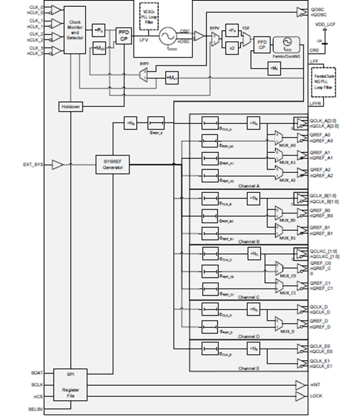
The 8V19N490-19BDGI is a JESD204B/C clock jitter attenuator launched by (Renesas), featuring a two-stage PLL architecture. It is mainly used in scenarios with high requirements for clock accuracy, such as wireless base stations and communication equipment. The following are its core features:
High-performance clock RF-PLL, supporting JESD204B
Optimized for low phase noise: -150 DBC /Hz (800kHz offset; 245.76MHz clock
Integral phase noise: 52fs RMS (typical value, 12kHz - 20MHz)
Dual PLL architecture
The first-stage PLL with an external VCXO can attenuate clock jitter
Second-stage PLL with internal FemtoClock NG PLL: 1966.08MHz
There are six output channels, totaling 19 outputs, which are divided into:
Four JESD204B channels (device clock and SYSREF output), with two-channel, four-channel and six-channel outputs
One clock channel, two outputs
A VCXO output
Configurable integer clock divider
The supported clock output frequencies include: 2949.12, 1474.56, 983.04, 491.52, 245.76, and 122.88
The low-power LVPECL/LVDS output supports configurable signal amplitudes, DC and AC coupling, as well as LVPECL and LVDS line termination technologies
Phase delay circuit
Clock phase delay, 256 steps 339ps, range 0 to 86.466ns
Independent SYSREF phase delay with eight levels of 169ps
An additional single SYSREF fine phase delay with a step size of 25ps
Global SYSREF signal delay, 256 steps 339ps, range 0 to 86.466ns
The redundant input clock architecture has four input terminals, including:
Input activity monitoring
Manual and automatic, fault-triggered clock selection modes
Priority control of clock selection
Digital hold and uninterrupted switching
The differential input accepts LVDS and LVPECL signals
The SYSREF generation mode includes both the internal and external trigger modes of JESD204B
Supply voltage: 3.3V
SPI and control I/O voltage: 1.8V/3.3V (optional)
Package: 11 x 11 mm 100-CABGA

Overview
The 8V19N490-19BDGI is a fully integrated FemtoClock® NG jitter attenuator and clock synthesizer, a high-performance clock solution for conditioning and frequency/phase management of radio equipment boards in wireless base stations. The 8V19N490-19BDGI has been optimized to offer outstanding phase noise performance, meeting the requirements of GSM, WCDMA, LTE and LTE-A radio board implementations. This device supports JESD204B subclass 0 and 1 clocks.
The two-level PLL architecture supports jitter attenuation and frequency doubling. The first-level PLL is a jitter attenuator, which uses an external VCXO to achieve the best phase noise characteristics. The second-level PLL locks the VCXO-PLL output signal and synthesizes the target frequency.
The 8V19N490-19BDGI supports generating high-frequency clocks from the selected VCO and low-frequency synchronization signals (SYSREF). The SYSREF signal is internally synchronized with the clock signal. In addition, the 8V19N490-19BDGI also features a delay function, which can adjust and control the phase delay between the system reference signal and the clock signal, and can adjust/delay individual output signals. Monitor the activities of the four redundant input terminals. The 8V19N490-19BDGI offers four optional clock switching modes for handling clock input failure situations. The automatic locking, separately programmable output divider and phase adjustment functions have been added to enhance flexibility. The 8V19N490-19BDGI is configured via a three-wire SPI interface and reports the locked and signal loss status through internal registers and LOCK detection (LOCK) output. Internal status bit changes can also be reported through nINT output. The 8V19N490-19BDGI is an ideal choice for driver converter circuits in wireless infrastructure, radar/imaging, and instrument/medical applications.
Typical applications
▪ Wireless infrastructure applications: GSM, WCDMA, LTE, LTE-A
▪ An ideal clock driver for jitter sensitive ADC and DAC circuits
▪ Low-phase noise clock generation
▪ Ethernet card
▪ Radar and imaging
▪ Instrumentation and medical care
Welcome to contact Mingjiada (www.hkmjd.com) for 8V19N490-19BDGI exclusive quote!
![[TI] INA193AIDBVR 500kHz Current Sense Amplifiers——Current Shunt Monitor](/upload/202508/25/202508251455390711.jpg)
Time:2025-08-25
![[Genuine Original Product] Infineon IGBT Module_FZ900R12KE4_1200V/900A Industrial Grade](/upload/202508/25/202508251435528213.jpg)
Time:2025-08-25

Time:2025-08-25

Time:2025-08-25
Contact Number:86-755-83294757
Enterprise QQ:1668527835/ 2850151598/ 2850151584/ 2850151585
Business Hours:9:00-18:00
E-mail:sales@hkmjd.com
Company Address:Room1239, Guoli building, Zhenzhong Road, Futian District, Shenzhen, Guangdong
CopyRight ©2022 Copyright belongs to Mingjiada Yue ICP Bei No. 05062024-12

Official QR Code
Links: