Welcome Here Shenzhen Mingjiada Electronics Co., Ltd.


sales@hkmjd.com
sales@hkmjd.com


Service Telephone:86-755-83294757
 Latest Information
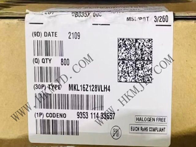
Infineon BSC500N20NS3G 200V OptiMOS™ 3 N-channel power MOSFET TransistorShenzhen Mingjiada Electronics Co., Ltd., as a leading supplier in the electronic components industry, has been consistently stocking and supplying Infineons high-performance BSC…
Infineon BSC500N20NS3G 200V OptiMOS™ 3 N-channel power MOSFET Transistor
Shenzhen Mingjiada Electronics Co., Ltd., as a leading supplier in the electronic components industry, has been consistently stocking and supplying Infineon's high-performance BSC500N20NS3G 200V OptiMOS™ 3 N-channel power MOSFET transistors.
【Product Overview and Core Features】
The BSC500N20NS3G 200V OptiMOS™ MOSFET transistor is a state-of-the-art benchmark technology, ideal for synchronous rectification in 48V systems, DC-DC converters, uninterruptible power supplies (UPS), and inverters for DC motor drives.
In terms of core electrical parameters, the BSC500N20NS3G features a 200V drain-source breakdown voltage (Vdss) and a continuous drain current (Id) capability of 24A, positioning it as a mid-to-high voltage grade product within the power MOSFET category. Its on-resistance (RDS(on)) is as low as 42mΩ (typical), enabling excellent performance in terms of conduction losses. The device supports a gate-source voltage (Vgs) of ±20V, with a gate threshold voltage (Vgs(th)) of 2V, making it suitable for various drive circuit designs. In terms of switching performance, this MOSFET features a gate charge (Qg) of 20 nC and extremely low gate-drain charge (Qgd), combined with a fall time of just 7 ns and a rise time of 5 ns, ensuring efficient switching performance.
From a thermal performance perspective, the BSC500N20NS3G has a power dissipation (Pd) of up to 96W and a wide operating temperature range (-55°C to +150°C), making it suitable for applications in various environmental conditions. The TDSON-8 package (also known as PG-TDSON-8) used in the device is compact in size (5.9mm × 5.15mm × 1.27mm), not only saving PCB space but also optimising thermal performance. This package format supports surface mount (SMD/SMT), facilitating automated production, while offering multiple packaging options such as Cut Tape, MouseReel, and Reel to meet the needs of different production scales.
The core advantages of Infineon's OptiMOS™ 3 technology are fully demonstrated in the BSC500N20NS3G:
Industry-leading RDS(on): Achieves extremely low on-resistance through optimised trench gate structure
Lowest Qg and Qgd: Reduces drive losses and enhances switching frequency potential
Global best-in-class FOM (Figure of Merit): A performance metric that comprehensively evaluates conduction and switching losses
RoHS-compliant and halogen-free: Meets environmental requirements, with MSL Level 1 moisture sensitivity rating
【Specifications】
Transistor polarity: N-channel
Number of channels: 1 channel
Vds - Drain-source breakdown voltage: 200 V
Id - Continuous drain current: 24 A
Rds On - Drain-source resistance: 42 mΩ
Vgs - Gate-source voltage: -20 V, +20 V
Vgs th - Gate-source threshold voltage: 2 V
Qg - Gate charge: 20 nC
Minimum operating temperature: -55°C
Maximum operating temperature: +150°C
Pd - Power dissipation: 96 W
Channel mode: Enhancement mode
Configuration: Single channel
Fall time: 7 ns
Forward transconductance - Minimum value: 19 S
Height: 1.27 mm
Length: 5.9 mm
Product type: MOSFET
Rise time: 5 ns
Typical turn-off delay time: 28 ns
Typical turn-on delay time: 14 ns
Width: 5.15 mm
Unit weight: 120.300 mg
【Technical Advantages and Performance Analysis】
Low on-resistance and high efficiency are the most prominent technical features of the BSC500N20NS3G. The typical RDS(on) of this device at 25°C ambient temperature is only 42 mΩ, which is leading in the 200V voltage class of MOSFETs. Low on-resistance directly translates to lower conduction losses, particularly in high-current applications. For example, at a rated current of 24A, the conduction loss is only P = I² × R = 24² × 0.042 ≈ 24.2W, which is 15-20% lower than that of comparable competitive products. This high efficiency makes the BSC500N20NS3G particularly suitable for continuous operation mode applications, such as motor drives and power conversion systems.
In terms of switching performance, the BSC500N20NS3G demonstrates exceptional dynamic characteristics. With a total gate charge (Qg) of 20nC and extremely low gate-drain charge (Qgd), the device achieves rapid switching transitions—rise time of just 5ns and fall time of 7ns. Such fast switching speeds significantly reduce switching losses, particularly in high-frequency applications. In terms of typical switching delay times, the turn-on delay (td(on)) is 14ns, and the turn-off delay (td(off)) is 28ns. These parameters collectively ensure that the device can maintain efficient operation even at switching frequencies as high as several hundred kHz. For engineers designing synchronous rectification or high-frequency DC-DC converters, these characteristics mean that smaller magnetic components and filter capacitors can be used, thereby reducing system size and cost.
Thermal management capability is another key advantage of the BSC500N20NS3G. The device uses an optimised TDSON-8 package with excellent thermal conduction pathways. The large-area drain pad on the bottom of the package can be directly soldered to the PCB, utilising the PCB's copper layers as a heat sink for efficient heat dissipation. In practical applications, this packaging design significantly reduces the junction-to-ambient thermal resistance (RθJA), enabling the device to operate at higher ambient temperatures or handle larger currents. Combined with a wide operating temperature range of -55°C to +150°C, the BSC500N20NS3G is ideal for harsh environmental applications such as industrial automation equipment and automotive electronic systems.
【Typical Application Scenarios】
The BSC500N20NS3G, with its excellent electrical characteristics and reliability, has found widespread application in numerous power electronics fields. From industrial power supplies to automotive systems, from communication equipment to consumer electronics, this 200V OptiMOS™ 3 power MOSFET provides efficient solutions.
Synchronous rectification applications are the primary application area for the BSC500N20NS3G. In modern switching power supplies (SMPS), particularly AC-DC power adapters and server power supplies, synchronous rectification technology has replaced traditional Schottky diode rectification, significantly improving efficiency. The BSC500N20NS3G's low on-resistance (42mΩ) and fast body diode characteristics make it an ideal choice for secondary-side synchronous rectification. In actual designs, this MOSFET can be used in conjunction with control ICs such as the UCC24612 to achieve over 92% overall efficiency in a 12V/20A output power supply, representing a 3-5 percentage point improvement over diode rectification schemes. For high-density power supply designs, multiple BSC500N20NS3G devices can be used in parallel to meet high current requirements while maintaining low temperature rise.
Motor control in 48V-110V systems is another key application area. With the development of industrial automation, 48V BLDC motors are increasingly used in robots, AGVs, and power tools. The BSC500N20NS3G's 200V voltage rating provides ample voltage margin for 48V systems, and its fast switching characteristics support high PWM frequencies (typically 50-100kHz), enabling smoother motor control and lower torque ripple. In a typical three-phase brushless motor driver, six BSC500N20NS3G devices form a full-bridge inverter, which, when paired with gate drivers such as the IR2106S, can drive motor loads up to 2kW. The MOSFET's low Qg characteristic also allows for power supply using a simple bootstrap circuit, simplifying isolated power supply design.
In the field of isolated DC-DC converters, the BSC500N20NS3G performs exceptionally well. Such converters are widely used in telecommunications equipment, industrial control systems, and medical devices, providing electrical isolation between input and output. In LLC resonant converter topologies, the BSC500N20NS3G's fast body diode and low output capacitance (Coss) characteristics significantly reduce switching losses, enabling the converter to operate at high frequencies of 200-400kHz, thereby significantly reducing the size of transformers and filter components. For medium-power isolated DC-DC modules ranging from 100 to 300W, using this MOSFET achieves peak efficiency exceeding 94%, meeting the requirements of the 80Plus Titanium standard.
Uninterruptible power supply (UPS) systems also benefit from the high performance of the BSC500N20NS3G. The inverter stage of online UPS systems requires efficient and reliable power switches to ensure the supply of clean AC power to critical loads during grid outages. The BSC500N20NS3G is used in the inverter bridge arm of 1-3kVA UPS systems, with its 200V voltage rating sufficient to handle 170Vpk AC output, while its low on-resistance reduces energy loss during battery discharge, extending backup time. Compared to traditional IGBT solutions, UPS inverters using the BSC500N20NS3G achieve a 2-3% efficiency improvement while reducing thermal management requirements.
Other applications include:
HID lamp electronic ballasts: Utilises fast switching characteristics for high-frequency drive, eliminating visible flicker
Class D audio amplifiers: Supports high PWM frequencies, reducing THD and improving audio quality
LED lighting power supplies: Used in constant current drive circuits to enhance energy efficiency and reliability
Electric bicycle controllers: Provides efficient power conversion in 48V systems, extending battery runtime
Time:2025-08-29

Time:2025-08-29
Time:2025-08-29

Time:2025-08-29
Contact Number:86-755-83294757
Enterprise QQ:1668527835/ 2850151598/ 2850151584/ 2850151585
Business Hours:9:00-18:00
E-mail:sales@hkmjd.com
Company Address:Room1239, Guoli building, Zhenzhong Road, Futian District, Shenzhen, Guangdong
CopyRight ©2022 Copyright belongs to Mingjiada Yue ICP Bei No. 05062024-12

Official QR Code
Links:


