Welcome Here Shenzhen Mingjiada Electronics Co., Ltd.

sales@hkmjd.com

sales@hkmjd.com

Service Telephone:86-755-83294757
 Latest Information
 Home
/Industry Information
/
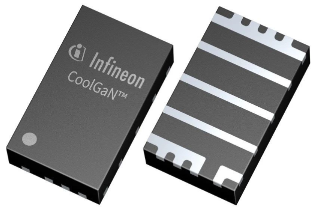
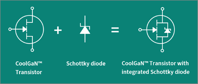
World's First! Infineon Introduces Industrial GaN FETs with Integrated SBDs
Recently吃, which improves the performance of the power system by reducing unnecessary deadband losses and further enhances overall system efficiency. In addition, the integrated solution simplifies power stage design and reduces cost of materials.The…
Recently吃, which improves the performance of the power system by reducing unnecessary deadband losses and further enhances overall system efficiency. In addition, the integrated solution simplifies power stage design and reduces cost of materials.

The integration of SBDs in power transistors has previously been the subject of a number of industry studies in SiC MOSFETs. Mitsubishi filed a patent related to SiC MOSFETs with integrated SBDs in 2013 and is launching SiC power modules with this new device in 2023.
Why integrate SBD into SiC MOSFETs?The PN junction between the source (Source) and drain (Drain) in the MOSFET structure will naturally form a body diode, which, as a by-product of the MOSFET structure, can provide protection for the MOSFET and improve reliability through rational design. However, the reverse recovery characteristics of the body diode is poor, as well as the body diode's long time conduction caused by the reliability problems, in practice, often in the external reverse parallel SBD as a continuation channel.
However, in order to improve integration, as well as to avoid the introduction of more parasitic capacitance inductance, so the integration of the SBD into the SiC MOSFET has become a direction.

Then for GaN FETs, Infineon explains that in hard-switching applications, GaN-based topologies may incur higher power losses due to the larger effective body diode voltage (VSD) of GaN devices. This is exacerbated if the controller has a long dead time, resulting in lower than target efficiency. Currently power device design engineers usually need to either connect an external Schottky diode in parallel with the GaN transistor, or shorten the dead time through the controller. However, either method requires additional effort, time and cost.
Integrating an SBD into a GaN transistor can therefore significantly solve these problems. Due to the lack of a body diode, the reverse conduction voltage (VRC) of a GaN transistor depends on the threshold voltage (VTH) and the gate bias voltage (VGS) in the off state. In addition, the VTH of GaN transistors is usually higher than the conduction voltage of silicon diodes, which results in a disadvantage during reverse conduction operation (also known as the third quadrant). As a result, with this new CoolGaN transistor, reverse conduction losses are reduced, compatibility with more high-side gate drivers is achieved and controller compatibility becomes wider due to the relaxed dead time, significantly simplifying design.
According to Infineon, the first GaN FET with integrated SBD is a 100V 1.5mΩ, E-Mode normally closed product in a 3 x 5 mm PQFN package for applications such as data centre IBCs, motor drives, DC-DC, chargers and more.
With the trend of high efficiency, miniaturisation and intelligence in power electronic systems, the integration of power devices is further accelerating to the ground. Mitsubishi in the last year has been introduced to the market 3kV SBD embedded SiC MOSFET module, and Infineon integrated SBD GaN transistors, and now also began to provide engineering samples, I believe that the future will continue to appear more new devices.
![[Supply] OPA2991SIRUGR (TI) 40V Dual Channel Low Noise Operational Amplifier](/upload/202508/16/202508161217045262.jpg)
Time:2025-08-16

Time:2025-08-16

Time:2025-08-16

Time:2025-08-16
Contact Number:86-755-83294757
Enterprise QQ:1668527835/ 2850151598/ 2850151584/ 2850151585
Business Hours:9:00-18:00
E-mail:sales@hkmjd.com
Company Address:Room1239, Guoli building, Zhenzhong Road, Futian District, Shenzhen, Guangdong
CopyRight ©2022 Copyright belongs to Mingjiada Yue ICP Bei No. 05062024-12

Official QR Code
Links: