Welcome Here Shenzhen Mingjiada Electronics Co., Ltd.


sales@hkmjd.com
sales@hkmjd.com


Service Telephone:86-755-83294757
 Latest Information
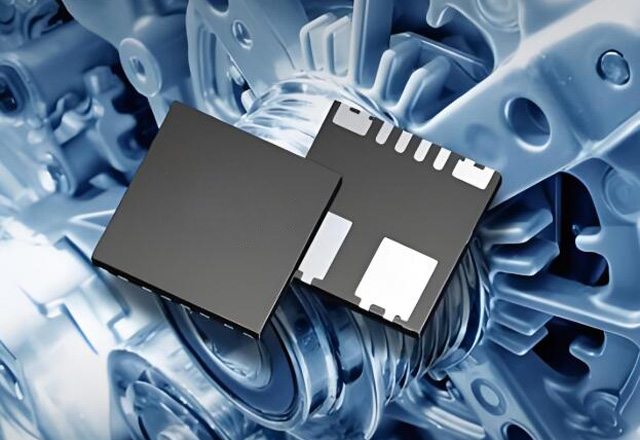
The AD7124-8WBBCPZ device is an 8-channel, low-noise, low-power, 24-bit Σ-Δ ADC that integrates PGA and reference voltage sources.InstructionsThe AD7124-8WBBCPZ is a low-power, low-noise, fully integrated analog front end for high-precision measurem…
The AD7124-8WBBCPZ device is an 8-channel, low-noise, low-power, 24-bit Σ-Δ ADC that integrates PGA and reference voltage sources.

Instructions
The AD7124-8WBBCPZ is a low-power, low-noise, fully integrated analog front end for high-precision measurement applications. The AD7124-8WBBCPZ Class W is AEC-Q100 certified for automotive applications. The device has a low-noise, 24-bit sigma-δ analog-to-digital converter (ADC) that can be configured to provide 8 differential inputs or 15 single-ended or pseudo-differential inputs. The low on-chip noise level ensures that small signals can be input directly into the ADC.
One of the main advantages of the AD7124-8WBBCPZ is the flexibility to use three integrated power modes. The current power consumption, output data rate range, and RMS noise can all be customized with the selected power mode. The device also offers multiple filter options, ensuring maximum flexibility for the user.
At an output data rate of 25 SPS (single-cycle build), the AD7124-8WBBCPZ can achieve both 50 Hz and 60 Hz rejection, and at lower output data rates, more than 80 dB rejection performance can be achieved.
The AD7124-8WBBCPZ offers the highest signal chain integration. The device incorporates a precision low-noise, low-drift internal bandgap reference voltage source and accepts an external differential reference voltage for internal buffering. Other key integrated features include a programmable low drift excitation current source, open test current control, and a bias voltage generator that sets the common mode voltage of a channel to AVDD/2. The low-end power switch allows the user to switch off the bridge sensor between transitions, ensuring the absolute minimum system power consumption. The device also allows users to work with an internal clock or an external clock.
In addition, the AD7124-8WBBCPZ integrates rich diagnostic capabilities as part of a comprehensive feature portfolio. These diagnostic capabilities include cyclic redundancy check (CRC), signal chain check, and serial interface check to provide a more robust solution. These diagnostic functions reduce the need for external components to perform diagnostic functions, which reduces the need for board space, reduces design time and saves costs. According to IEC 61508, Failure Mode Impact and Diagnostic Analysis (FMEDA) for typical applications indicates a safe failure ratio (SFF) greater than 90%.
The AD7124-8WBBCPZ has the following features:
3 power consumption modes
RMS noise
Low power consumption: 24 nV rms (1.17 SPS), gain =128 (typical 255 μA)
Medium power: 20 nV rms (2.34 SPS), gain =128 (typical 355 μA)
Full power: 23 nV rms (9.4 SPS), gain =128 (typical 930 μA)
Noise-free resolution up to 22 bits (gain =1) in all power modes
Output data rate
Full power: 9.38 SPS to 19,200 SPS
Medium power: 2.34 SPS to 4800 SPS
Low power consumption: 1.17 SPS to 2400 SPS
Rail-to-rail analog input (gain greater than 1)
50 Hz/60 Hz simultaneous rejection (25 SPS, single cycle establishment)
Diagnostic capabilities (for safety Integrity Level (SIL) certification)
Cross point multiple analog inputs
8 differential /15 pseudo-differential inputs
Programmable gain (1 to 128)
Bandgap reference voltage source with a maximum drift of 10 ppm/°C (70 μA)
Programmable matching excitation current
Internal clock oscillator
On-chip bias voltage generator
Low power switch
Universal output
Multiple filter options
Internal temperature sensor
Self-calibration and system calibration
Sensor open circuit detection
Automatic channel timing controller
Each channel is configured independently
Power supply: 2.7 V to 3.6 V and ±1.8 V
Independent interface power supply
Turn-off current: 5μA (Max)
Temperature range: −40°C to +125°C
32-pin LFCSP package
3 - or 4-wire serial interface
SPI, QSPI™, MICROWIRE™ and DSP compatible
Schmidt trigger in SCLK pin
ESD: 4 kV
Passed AEC-Q100 Automotive application certification
Application field
The AD7124-8WBBCPZ is widely used in high precision measurement, industrial control, medical instruments and sensor interfaces. Its high accuracy, low noise and low power consumption make it excellent in applications where accurate data acquisition is required .

Contact us
For [AD7124-8WBBCPZ analog to digital converter] sample or purchase services, you can visit the official website www.hkmjd.com contact Mingjiada Electronics.
Time:2025-07-08
Time:2025-07-08
Time:2025-07-08
![Supply [Infineon] AIROC™ Wi-Fi Connected MCU, AIROC™ Bluetooth LE, Wi-Fi 6 Combo](/upload/202507/08/202507081447596589.jpg)
Time:2025-07-08
Contact Number:86-755-83294757
Enterprise QQ:1668527835/ 2850151598/ 2850151584/ 2850151585
Business Hours:9:00-18:00
E-mail:sales@hkmjd.com
Company Address:Room1239, Guoli building, Zhenzhong Road, Futian District, Shenzhen, Guangdong
CopyRight ©2022 Copyright belongs to Mingjiada Yue ICP Bei No. 05062024-12

Official QR Code
Links:


