Welcome Here Shenzhen Mingjiada Electronics Co., Ltd.


sales@hkmjd.com
sales@hkmjd.com


Service Telephone:86-755-83294757
 Latest Information
Recently, Lattice announced its forward-looking placement in FPGA design, enabling it to incorporate MRAM technology with a number of innovative products including Certus-NX, CertusPro-NX and Avant. These FPGA devices feature optimised architectural d…
Recently, Lattice announced its forward-looking placement in FPGA design, enabling it to incorporate MRAM technology with a number of innovative products including Certus-NX, CertusPro-NX and Avant. These FPGA devices feature optimised architectural designs and proven process technologies with built-in hard erasers, error detection and correction mechanisms, providing users with a reliable development environment. With the latest Radiant tools, users can directly implement MRAM programming interfaces to support a wide range of storage capacities and data rates. With these FPGA devices, users can benefit from low-power FPGA architectures and fast and secure bitstream configuration/reconfiguration.
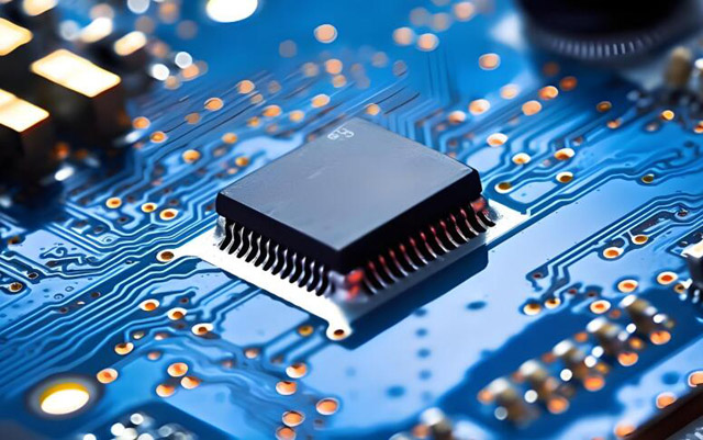
Designing a circuit or application for an FPGA requires the use of a hardware description language (HDL) to describe how the functions within the FPGA should be wired.The HDL code is compiled into an FPGA configuration file, known as a bitstream, using FPGA development software. The bitstream contains binary data that tells each logic element (flip-flop, gate, etc.) inside the FPGA how to connect and perform digital functions. Once generated, the bitstream is stored in a non-volatile memory device. The configuration bitstream is loaded into the FPGA during the power-up process. Once the bitstream is configured, the FPGA begins to perform any of a variety of programming tasks, such as data or signal processing, control functions and protocol bridging.
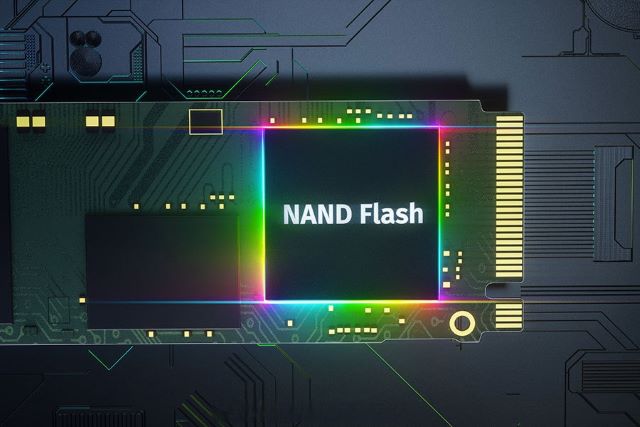
FPGAs previously relied heavily on flash memory to store configuration bitstreams, Lattice said. This approach worked for many mainstream FPGA configuration applications; however, as technology advances and the need for higher reliability and performance increases, there is a need for more diverse configuration storage options. The catalyst for this shift lies in the diverse needs of applications and industries, which are now pushing the limits of FPGA applications to go further in terms of data integrity, system endurance, and operational efficiency.
For example, in network edge applications requiring high endurance or performance, MRAM can handle a large number of high-speed read/write cycles via OTA to support continuous data updates without having to go through erase cycles and without the need for a flash file system or dedicated controller. Flash memory, while reliable under certain conditions, has limitations in terms of endurance.
In automotive applications, MRAM can operate efficiently over a wide temperature range and under harsh conditions. In mission-critical transport and avionics applications, MRAM is critical for storing records of system setup and operational data. In space applications where data reliability is critical, MRAMs are resistant to strong radiation, simplifying on-orbit reprogramming and limiting radiation-induced errors.
In time-critical environments such as real-time sensor data processing or high-reliability communications, the need for fast configuration is critical. Conventional flash memory causes delays in boot time.
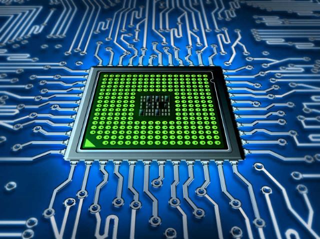
Magnetic Random Access Memory (MRAM) is an emerging non-volatile memory technology that uses the magnetic properties of materials to store data. Unlike traditional flash memory, which relies on charge storage, magnetic random access memory uses magnetic tunnel junctions to represent binary data as the direction of magnetic states. This approach offers several advantages, including lower power consumption, higher endurance, and faster read and write speeds. In addition, MRAM's non-volatility ensures that data is retained even in the absence of a power source, making it a reliable and efficient alternative to flash memory.
According to Lattice, the use of MRAM to store FPGA configuration bitstreams is not just a technology upgrade, but a strategic move towards future-proofing highly reliable systems. As industries continue to demand more from their electronic components, MRAM-enabled FPGA systems have become the optimal solution for failure-zero tolerance applications.
In the AI era, the characteristics of MARM can meet the needs of edge computing and is one of the ideal memories for storage-computing integration.MRAM is combined with AI chips to achieve storage-computing integration architecture and improve the operational efficiency of AI algorithms. For example, in the fields of image recognition, voice recognition, etc., AI chips with integrated memory-computing can achieve higher performance and lower power consumption.
MRAM is based on the control of electronic ‘spin’, can reach the theoretical zero static power consumption, at the same time has a high speed and non-volatile and nearly unlimited number of writes, MRAM in the speed, durability, power consumption of these aspects have irreplaceable superiority.
MRAM is also integrated with other storage technologies, such as combining MRAM with DRAM and flash memory, etc. In mobile devices, MRAM can be used as a cache, and DRAM and Flash form a hybrid storage system to improve the performance and endurance of the device. Taking advantage of various storage technologies to achieve the best balance of performance, capacity and cost.
Time:2025-08-08
Time:2025-08-08
Time:2025-08-08
Time:2025-08-08
Contact Number:86-755-83294757
Enterprise QQ:1668527835/ 2850151598/ 2850151584/ 2850151585
Business Hours:9:00-18:00
E-mail:sales@hkmjd.com
Company Address:Room1239, Guoli building, Zhenzhong Road, Futian District, Shenzhen, Guangdong
CopyRight ©2022 Copyright belongs to Mingjiada Yue ICP Bei No. 05062024-12

Official QR Code
Links:


